Just got around to perform a little test that I've been wanting to try for quite some time now. Most (if not all?) chip amps state in their datasheets that the closed loop gain has to be larger than 20dB or 24dB for the amplifier to run stable. However, I can think of several use cases where I don't need that much gain, so I tried to get rid of several dB's using noise gain compensation. Here's a nice article on the subject: Compensating Amplifiers That Are Stable at Gain = 10 to Operate at Lower Gains | Analog Devices.
In short: Op amps have a signal gain and a noise gain, which are equal to each other in most cases. The stability of the op amp is dependent on the noise gain, which lets us set the signal gain to 6dB for example, while at the same time the noise gain is set to 27dB to keep the amp stable.
This freedom comes at a price, of course. From what I've read so far, the noise gain is called like this, because it increases the gain of the input noise. Interestingly I've made the exact opposite observation....
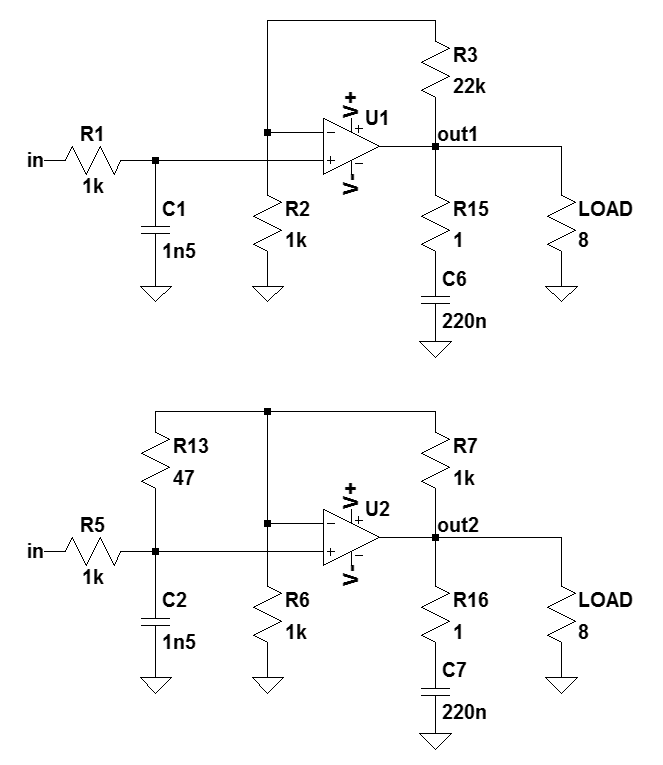
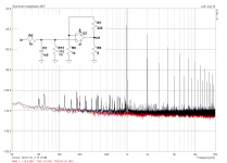
I started out building a small test circuit with a TDA2030A running at stabilized +-15V and a resistive 8R or 100R load. The circuit is close to the datasheet example, using 22k and 1k in the feedback loop for ~27dB gain. The noise gain version uses 1k and 1k for 6dB gain, with an additional 47R between the op amp inputs. Signal gain is (1k/1k)+1 = 2 (6dB) while noise gain is (1k/1k||47)+1 = 23,3 (27,3dB).
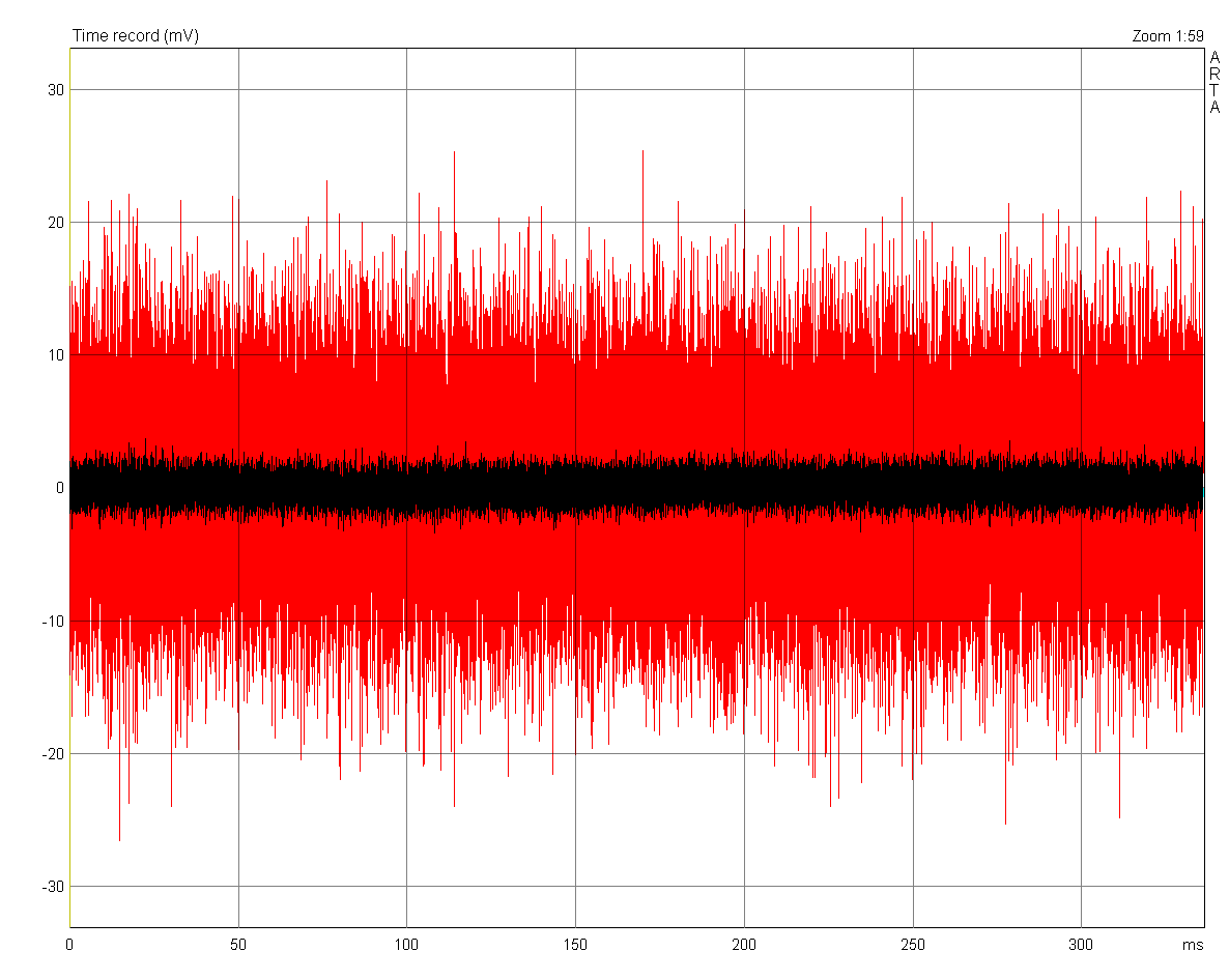
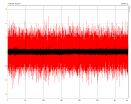
The most obvious and most useful difference is the output noise. The 6dB circuit (black trace) is a lot quieter. I didn't expect that, tbh. Not sure if the 27dB circuit (red trace) is actually oscillating, but I couldn't find any traces with my 100MHz scope to confirm that. Tested with 8R and 100R resistive load for no difference.
And now for the downsides . The output offset is huuuge! With the 27dB configuration I measured around 100mV, which can be brought down a bit more by using a capacitor in the feedback path. The 6dB circuit sits at a whopping 3V at the output, which is basically unusable without an output cap. Adding an input cap and a feedback cap brought this down to around 700mV, which is still a lot.
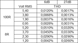
The other thing is that the total harmonic distortion with the 6dB version is noticeably higher. Seems plausible, because now there's not a lot of feedback left to bring it down.
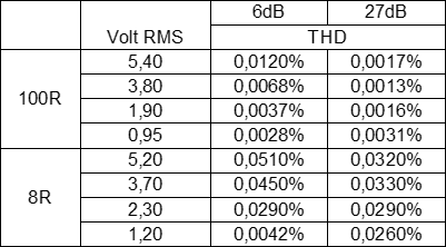
The 6dB circuit might actually be useable as a headphone amplifier. It has to be capacitor coupled at the output, but then again that might enable it to run from a single rail only. Due to the high output offset the amp is actually running in Class A for small output swings! You can see that in the THD table for the values around 1VRMS, where the 6dB version has lower THD than the standard 27dB version, especially into 8R.
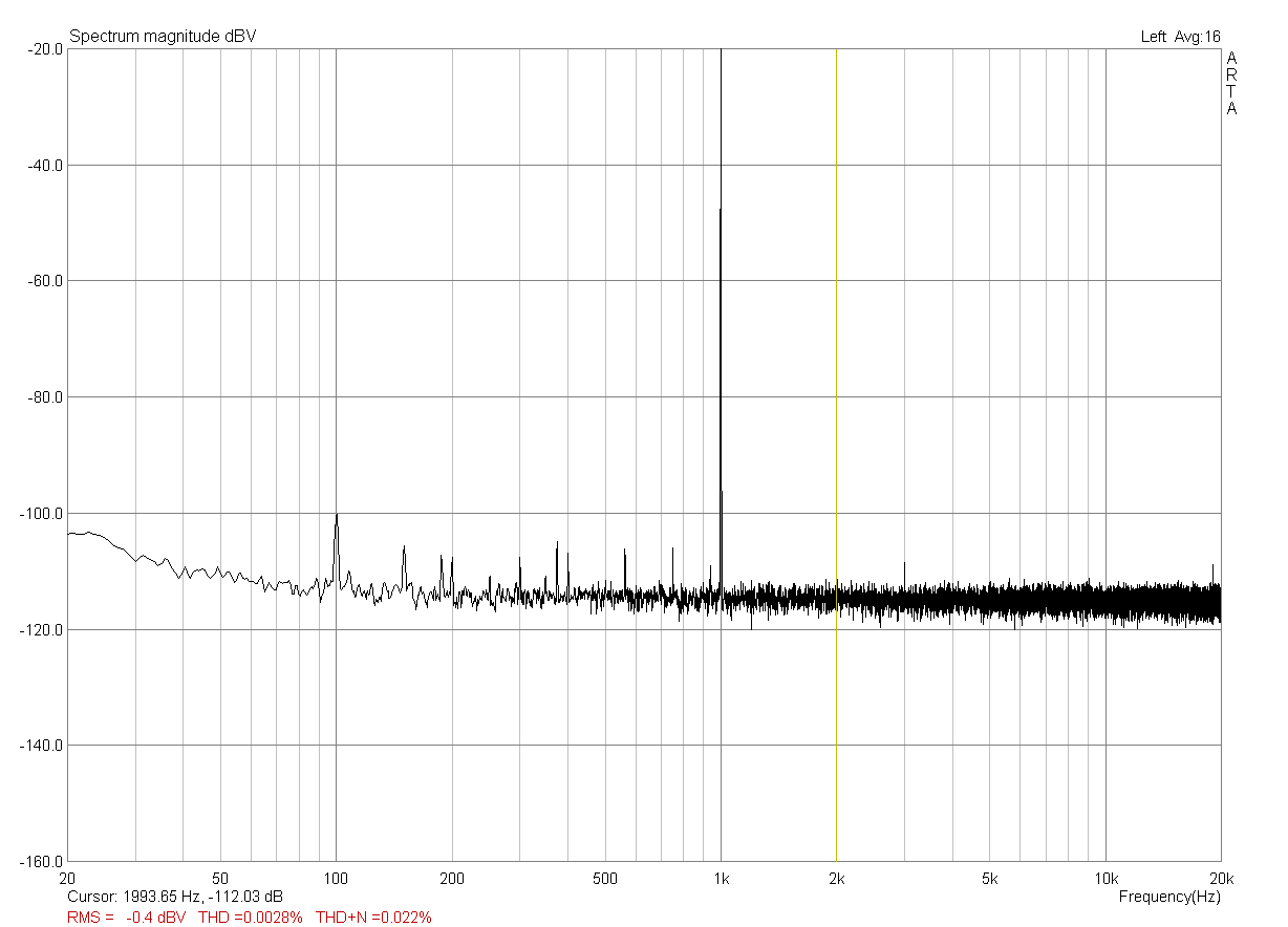
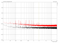
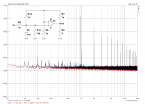
This is the spectrum for the 6dB circuit running 0,95VRMS into 100R. The second and third harmonic sit at -112dBV, while the rest is hidden in the noise floor.
I think I have an LM1876 somewhere in the parts bin, maybe I'll give that one a try up next...
.
In short: Op amps have a signal gain and a noise gain, which are equal to each other in most cases. The stability of the op amp is dependent on the noise gain, which lets us set the signal gain to 6dB for example, while at the same time the noise gain is set to 27dB to keep the amp stable.
This freedom comes at a price, of course. From what I've read so far, the noise gain is called like this, because it increases the gain of the input noise. Interestingly I've made the exact opposite observation....
I started out building a small test circuit with a TDA2030A running at stabilized +-15V and a resistive 8R or 100R load. The circuit is close to the datasheet example, using 22k and 1k in the feedback loop for ~27dB gain. The noise gain version uses 1k and 1k for 6dB gain, with an additional 47R between the op amp inputs. Signal gain is (1k/1k)+1 = 2 (6dB) while noise gain is (1k/1k||47)+1 = 23,3 (27,3dB).
The most obvious and most useful difference is the output noise. The 6dB circuit (black trace) is a lot quieter. I didn't expect that, tbh. Not sure if the 27dB circuit (red trace) is actually oscillating, but I couldn't find any traces with my 100MHz scope to confirm that. Tested with 8R and 100R resistive load for no difference.
And now for the downsides
. The output offset is huuuge! With the 27dB configuration I measured around 100mV, which can be brought down a bit more by using a capacitor in the feedback path. The 6dB circuit sits at a whopping 3V at the output, which is basically unusable without an output cap. Adding an input cap and a feedback cap brought this down to around 700mV, which is still a lot.The other thing is that the total harmonic distortion with the 6dB version is noticeably higher. Seems plausible, because now there's not a lot of feedback left to bring it down.
The 6dB circuit might actually be useable as a headphone amplifier. It has to be capacitor coupled at the output, but then again that might enable it to run from a single rail only. Due to the high output offset the amp is actually running in Class A for small output swings! You can see that in the THD table for the values around 1VRMS, where the 6dB version has lower THD than the standard 27dB version, especially into 8R.
This is the spectrum for the 6dB circuit running 0,95VRMS into 100R. The second and third harmonic sit at -112dBV, while the rest is hidden in the noise floor.
I think I have an LM1876 somewhere in the parts bin, maybe I'll give that one a try up next...
.
Attachments


Last edited:
I suspect oscillation.
The way it is usually done for audio is with the cap. You only need gain>26dB above the second pole around a half MHz. The values below give 6dB 0-30kHz rising to 26dB above 500kHz.
_I_ think 1.5nFd hung on the input is excessive. Many systems won't mind, some will. The 1k takes some of the load off, true.
Attachments

Ok you have less noise , but with a gain of 6db you must add another op amp to have necessary sensitivity. What than would be the result . You can also try inverting mode but instead of having just a resistor to the input, to fix the gain 6db you put a RCR T to let the circuit see the gain at high frequencies equal to 20db and at low 6db.
I would say that by reducing the impedance level around the inputs, especially by shunting them directly with 47 ohm you practically eliminate all of the noise current, which is probably dominant in the case of this chipThis freedom comes at a price, of course. From what I've read so far, the noise gain is called like this, because it increases the gain of the input noise. Interestingly I've made the exact opposite observation....
.
This. If bringing down the gain brings down the noise, your noise source is essentially part of the input signal.Its worth comparing with a 3rd configuration, input -20dB attenuator into 26dB gain version - with similar input impedance as the 6dB version.
With impedances in the order of 1k, that would have to be one heck of a lot of current noise. Your input transistors would have to run at close to 2 mA a pop to even get to 1.6 pA/√(Hz).I would say that by reducing the impedance level around the inputs, especially by shunting them directly with 47 ohm you practically eliminate all of the noise current, which is probably dominant in the case of this chip
Specs for the TDA2030 say 3 µV and 80 pA, 22-22k Hz, typ - that works out to 20 nV/√(Hz) and 0.5 pA/√(Hz), respectively. You'd definitely have to get into the dozens of kOhms for current noise to become an issue.
In this case IC input noise is probably dominated by measurement soundcard output noise. 3 µV @22k is about the equivalent of a 20k SNR of 117 dB ref: 2V or 111 dB ref: 1 V - that's Xonar D2 terrain.
Last edited:
1.6pA/√Hz would be 8µA bias, not 2mA - an amp with simple input pair would be somewhere in that region, I think the TDA2030 must be darlington inputs or 3-stage.
The datasheet conflates flicker noise with voltage and current noise values, but I don't think flicker can be a big problem given the graphs.
The datasheet conflates flicker noise with voltage and current noise values, but I don't think flicker can be a big problem given the graphs.
There aren't many references to audio chipamp schematics and even fewer details online but TDA2030 at least, has an equivalent schematic published originally by Telefunken, when they were making semis. Indeed, it shows Darlington inputs. Datasheet Archive TDA2030 datasheet download
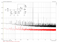
Only had time for a quick test yesterday and noticed something embarrassing: I accidentally omitted a solder joint on the vero board and thus the 1n5 cap at the input was not connected to ground! Fixed that and ran 3.7VRMS into 8R again. The 27dB version was the same within the margin of error, but the 6dB version actually increased substantially. The output offset disappeared, the noise floor got even lower and THD went from 0.045% to 0.0053%. I'll investigate that further at the weekend.
OK, I think I've found another mistake that I made. I'm using an ESI Juli@ sound card for the measurements and have it configured to use the symmetrical interface to avoid ground loops. Unfortunately the output impedance seems to be a little on the high side when using it on a single-ended input, thus the non-inverting input didn't have a sufficient path to ground, resulting in the rather high dc offsets. To fix this, I have now added an arbitrarily chosen 10k from the non-inverting input to ground.
The now fixed 10k input impedance however did nothing to increase the noise floor of the standard circuit. It still remains highest of them all. The output offset is still around 70mV, roughly halved to 1.25V for the second circuit and is basically zero for the third circuit.
The much better THD results that I reported yesterday actually came from the third circuit, which is about what PRR suggested. Instead of 47R and 1nF I used 47R and 4n7, because that was what I had handy. Notice that the noise floor of the third circuit is even lower than that of the second one, and the THD in this case increased by a whole order of magnitude!
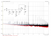
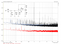
The black trace shows the distortion measurement at 1kHz with ~3.3VRMS into 8R. The blue trace shows the noise floor with no soundcard output (ARTA generator set to External). The red trace shows the noise floor with the input shorted directly at the amplifier vero board, but the soundcard output still connected and muted (set to External again).
The now fixed 10k input impedance however did nothing to increase the noise floor of the standard circuit. It still remains highest of them all. The output offset is still around 70mV, roughly halved to 1.25V for the second circuit and is basically zero for the third circuit.
The much better THD results that I reported yesterday actually came from the third circuit, which is about what PRR suggested. Instead of 47R and 1nF I used 47R and 4n7, because that was what I had handy. Notice that the noise floor of the third circuit is even lower than that of the second one, and the THD in this case increased by a whole order of magnitude!
The black trace shows the distortion measurement at 1kHz with ~3.3VRMS into 8R. The blue trace shows the noise floor with no soundcard output (ARTA generator set to External). The red trace shows the noise floor with the input shorted directly at the amplifier vero board, but the soundcard output still connected and muted (set to External again).
Attachments
On the 3rd circuit, you have the R1/C1 connected wrong. It sould go to the '-' input, not the '+'.
But hey, this should be in the CHIPAMP forum!
You're twice right!
Just had to check again that I didn't hook this up wrong again, but the circuit is correct; just messed up the schematic. Here's the correct one.
Attachments

Messed up the schematic for the first circuit, too : R7 should read 22k, not 1k!
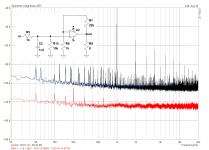
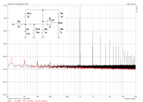
I have made another test with reduced feedback resistor values. This is the standard circuit with a 22k + 1k feedback network and a 1k + (1k||47R) network for roughly the same gain. Overall performance is virtually the same; THD is a little worse with the lower resistance, but that's within the margin of error I'd say.
: R7 should read 22k, not 1k!I have made another test with reduced feedback resistor values. This is the standard circuit with a 22k + 1k feedback network and a 1k + (1k||47R) network for roughly the same gain. Overall performance is virtually the same; THD is a little worse with the lower resistance, but that's within the margin of error I'd say.
Attachments
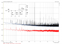
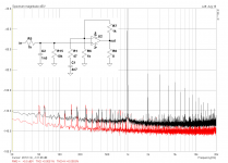
And another. Again the standard circuit with 22k + 1k, but this time with an additional 100R in parallel to the 10k at the non-inverting input to divide the input voltage down. Noise performance is still the same, but the THD skyrocketed due to the rather low input impedance.
In a second attempt I changed the input divider from 1k + (10k||100R) to 101k + 10k, which brought the overall performance back up to the level of the standard circuit.
So dividing down the input by 20dB and amplifying it up by 27dB afterwards doesn't bring any advantages in this case. The circuit as proposed by PRR on the other hand actually beats the standard circuit in terms of overall output noise level, THD, and output offset. The low gain of 6dB is of no problem, if a preceding preamp can put out 20Vpp with low noise and distortion, which would then be sufficient to saturate the TDA and drive it into its supply voltage limits.
Attachments
PRR's circuit is the standard method when you want to stabilize an amplifier requiring >1 amplification to be stable.The circuit as proposed by PRR on the other hand actually beats the standard circuit in terms of overall output noise level, THD, and output offset.
Why would you ruin the DC stability and the LF performance with a direct shunt of the inputs, when adding a capacitor gets you the best of both worlds (mostly).
Up to the pole created by the additional cap, you benefit from the supplementary loop gain, which explains the reduced THD and lower noise
With 20dB less gain, we expect 20dB less self-hiss (in band). And 20dB gain diverted to NFB suggests 1/10th the THD.
Allowing for rounding (and repeated mis-wires and poor drive), this is exactly what you observed. Any other result would be funny.
The self-noise goes up above the corner point. In this case that may be 30kHz so there may be a peak of 100kHz hiss (above the range of your sound card). This is why we don't do it more often. (Also the fact that the lost 20dB would typically have to be made-up with more stages; though some applications don't really need 26dB gain.)
PRR's circuit is the standard method when you want to stabilize an amplifier requiring >1 amplification to be stable.
Learning something new every day
. Never noticed this before.Why would you ruin the DC stability and the LF performance with a direct shunt of the inputs, when adding a capacitor gets you the best of both worlds (mostly).
Now that I've done this test, I wouldn't!
With 20dB less gain, we expect 20dB less self-hiss (in band). And 20dB gain diverted to NFB suggests 1/10th the THD.
Sounds reasonable now that you say it. I actually didn't expect this to work though...
The self-noise goes up above the corner point. In this case that may be 30kHz so there may be a peak of 100kHz hiss (above the range of your sound card). This is why we don't do it more often.
How bad could that possibly be? Normal tweeters probably don't go that high; ribbon tweeters might, but I don't think that would be audible anyway. The LPF at the input should take care of higher frequencies going in and thus reduce the risk of creating intermodulation distortion which might again be audible.
I re-ran the measurement with the soundcard configured for the single-ended interface. The overall noise floor is a bit lower now, but so is the input voltage range. Had to back up by 5dBV, because 10dBV would clip the soundcard input.
Attachments
- Status
- This old topic is closed. If you want to reopen this topic, contact a moderator using the "Report Post" button.
- Home
- Amplifiers
- Chip Amps
- Fun with a cheap TDA2030A at only 6dB gain