Hi all,
Currently, I am building a simple LM1875 based stereo amp for home and would highly appreciate feedback from the DIY audio community.
This is my very first build of a DIY amplifier and in parallel, I am learning to use KiCAD. I will be ordering PCBs hopefully soon and really afraid of any possible issues given my lack of experience is both CAD and circuitry design!
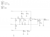
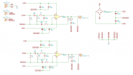
The schematic I am using is nothing short of a good ol' Silicon Chip Schoolies amp with a reference to those $2 eBay lm1875 kits - I just wanted to make something better and learn something new.
I will be using JLPCB to get both PCBs for both amp PCBs as well as the PSU PCBs and will be sourcing components from Digikey.
Small comments about the amp boards - as I mentioned, I tried to mimic the eBay kits - I found a lot of good feedback on that type of a layout.
I also kept the signal part separate from the high voltage components and tried to reduce the amount of traces running parallel. What is not present in the amp PCB is the shape fill - I removed it since it made all the legends and position of the component on the silkscreen unreadable. I hope shape fills help me to minimize the crosstalk if that is even a thing in that case.
I tried to select decent grade components for the board itself without going crazy about audio grade components. I do hope that a couple of extra $$ would help alleviate my infant hardware design skills")
I would highly appreciate the reviews of the schematic, PCBs and the BOM! if there is anything I can make do to get the layout better - more then happy to! First port in the community and hope, not the last one. Highly appreciate everyone's time!
Currently, I am building a simple LM1875 based stereo amp for home and would highly appreciate feedback from the DIY audio community.
This is my very first build of a DIY amplifier and in parallel, I am learning to use KiCAD. I will be ordering PCBs hopefully soon and really afraid of any possible issues given my lack of experience is both CAD and circuitry design!
The schematic I am using is nothing short of a good ol' Silicon Chip Schoolies amp with a reference to those $2 eBay lm1875 kits - I just wanted to make something better and learn something new.
I will be using JLPCB to get both PCBs for both amp PCBs as well as the PSU PCBs and will be sourcing components from Digikey.
Small comments about the amp boards - as I mentioned, I tried to mimic the eBay kits - I found a lot of good feedback on that type of a layout.
I also kept the signal part separate from the high voltage components and tried to reduce the amount of traces running parallel. What is not present in the amp PCB is the shape fill - I removed it since it made all the legends and position of the component on the silkscreen unreadable. I hope shape fills help me to minimize the crosstalk if that is even a thing in that case.
I tried to select decent grade components for the board itself without going crazy about audio grade components. I do hope that a couple of extra $$ would help alleviate my infant hardware design skills
I would highly appreciate the reviews of the schematic, PCBs and the BOM! if there is anything I can make do to get the layout better - more then happy to! First port in the community and hope, not the last one. Highly appreciate everyone's time!
Attachments
My only comment on the schematic would be the use of the feedback capacitor to ground. I assume this IS the safer approach regarding things blowing up and is easily bypassed in its spot in the etch layout, should you ever desire to do so.
My opinion is that this cap should be the highest quality you can muster. Better yet, no cap in accordance with a general first principle of audiophilia "The fewer caps in series with the signal path, the better". However bypassing it could be perilous and particularly as this is your first time out.
I'm currently listening to such an amplifier with the cap removed, feedback resistor to ground - and thoroughly enjoying the music. My amp has been power cycled multiple times with no smoke yet. I listen conservatively, rarely if ever taking the amp anywhere near its power output limits. Currently, I'm experimenting with different types of feedback, hoping to incorporate some current sensing into the equation and raising the output impedance of the amplifier, more closely resembling a tube amp.
Doing that takes advantage of the fact I never listen "as loud as it can go without distorting" which give me latitudes that wouldnt sell in commercially available product. I'm not trying for a design that pleases the broadest possible audience, results in the smallest number of returns and service calls, warranty issues - I'm trying for a design that pleases me.
A nice little amplifier! Paired with a tube preamp (or these days, tube buffered DAC) that has a little 2nd harmonic distortion, you should be into SET equivalent territory I dare say. Try some high efficiency point source FR speakers with it, if you can afford 'em! (That would take a few more caps out of the "digits to ears" signal path)
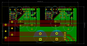
I've attached the schematic and PCB layout from Post #1 as images rather than PDFs to make them easier to see on the forum.
Depends a lot on the cap. The Nichicon UES-series of bipolar caps don't add any distortion that I can measure, and I find them to me sonically transparent as well.
The feedback cap (C3) could be larger. 22 uF, 1 kΩ gives you 7 Hz cutoff. I generally aim for 2 Hz (10x below the audio range) to avoid excessive rolloff within the audio band. I'd up C3 to 100 uF.
I'd up R3 to 47 kΩ (or C1 to 4.7 uF) for similar reasons.
These tweaks are minor, though.
R2 is more likely to degrade performance than it is to improve it. I suggest taking the ground reference at the speaker output ground as that's the voltage you care about. You can read my thoughts here: Grounding – Neurochrome
In general, I suggest you read the entire Taming the LM3886 series: Taming the LM3886 Chip Amplifier – Neurochrome
While the article series is aimed at the LM3886, 90+ % of the content applies equally to the other ICs in the Overture series, including the LM1875. In particular, I suggest reading the parts on grounding and power supply decoupling. You may find the page on Thermal Design helpful as well.
I don't mean to scare you off with all the "homework". I'm trying to set you up for success. The LM1875 is pretty easy going, but I think it helps to know a little about the common pitfalls in chipamp audio design, which is why I put that article series together.
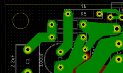
PCB Layout Review:
The layout is decent, though you're not making very good use of the available copper. Also, I suggest moving the decoupling caps much closer to the IC. C6 and C7 should be right at the pins. C2 and C4 shouldn't be far away either. Right now, C2 and C4 are lined up with the IC, which means you'll have a hard time getting a screwdriver in to mount the IC. I suggest placing them closer to the IC and off to the right by enough that you can get a screwdriver in.
I suggest making the power connections to the IC pours rather than traces. I also suggest using a ground plane. You're paying for the copper anyway, so you might as well make it work for you.
The trace to R6 runs perilously close to the edge of the board. You want 50 mil (0.050" = 1.25 mm) minimum from the edge of the trace to the edge of the board. Otherwise, the trace might disappear when the board is cut from the panel.
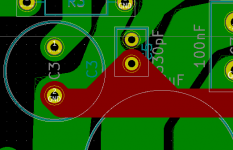
You have a couple of acid traps in your layout (marked in red). You want to avoid traces coming together at acute angles as it can result in over-etching. It's not as big of an issue in the professional fabs as it used to be, but if you plan to etch the board yourself, you could end up with broken traces.
Also, try to go straight into pads (weird pad exits marked in blue).
For a first-timer, you're doing really well so far, though.
Tom
My opinion is that this cap should be the highest quality you can muster. Better yet, no cap in accordance with a general first principle of audiophilia "The fewer caps in series with the signal path, the better".
Depends a lot on the cap. The Nichicon UES-series of bipolar caps don't add any distortion that I can measure, and I find them to me sonically transparent as well.
The feedback cap (C3) could be larger. 22 uF, 1 kΩ gives you 7 Hz cutoff. I generally aim for 2 Hz (10x below the audio range) to avoid excessive rolloff within the audio band. I'd up C3 to 100 uF.
I'd up R3 to 47 kΩ (or C1 to 4.7 uF) for similar reasons.
These tweaks are minor, though.
R2 is more likely to degrade performance than it is to improve it. I suggest taking the ground reference at the speaker output ground as that's the voltage you care about. You can read my thoughts here: Grounding – Neurochrome
In general, I suggest you read the entire Taming the LM3886 series: Taming the LM3886 Chip Amplifier – Neurochrome
While the article series is aimed at the LM3886, 90+ % of the content applies equally to the other ICs in the Overture series, including the LM1875. In particular, I suggest reading the parts on grounding and power supply decoupling. You may find the page on Thermal Design helpful as well.
I don't mean to scare you off with all the "homework". I'm trying to set you up for success. The LM1875 is pretty easy going, but I think it helps to know a little about the common pitfalls in chipamp audio design, which is why I put that article series together.
PCB Layout Review:
The layout is decent, though you're not making very good use of the available copper. Also, I suggest moving the decoupling caps much closer to the IC. C6 and C7 should be right at the pins. C2 and C4 shouldn't be far away either. Right now, C2 and C4 are lined up with the IC, which means you'll have a hard time getting a screwdriver in to mount the IC. I suggest placing them closer to the IC and off to the right by enough that you can get a screwdriver in.
I suggest making the power connections to the IC pours rather than traces. I also suggest using a ground plane. You're paying for the copper anyway, so you might as well make it work for you.
The trace to R6 runs perilously close to the edge of the board. You want 50 mil (0.050" = 1.25 mm) minimum from the edge of the trace to the edge of the board. Otherwise, the trace might disappear when the board is cut from the panel.
You have a couple of acid traps in your layout (marked in red). You want to avoid traces coming together at acute angles as it can result in over-etching. It's not as big of an issue in the professional fabs as it used to be, but if you plan to etch the board yourself, you could end up with broken traces.
Also, try to go straight into pads (weird pad exits marked in blue).
For a first-timer, you're doing really well so far, though.
Tom
Attachments

Last edited:
Hi Tom
you wrote:
The feedback cap (C3) could be larger. 22 uF, 1 kΩ gives you 7 Hz cutoff. I generally aim for 2 Hz (10x below the audio range) to avoid excessive rolloff within the audio band. I'd up C3 to 100 uF.
I'd up R3 to 47 kΩ (or C1 to 4.7 uF) for similar reasons.
if i use a 10µF at input cap + 100µF as C3 should a change something else?
i read through your hint about R2 but i am not sure i understand everything . as you can read in the prallel thread about the LM1875 kit should i cut the trace or what should i do with the R2 area to perform better?
thanks in advance
chris
you wrote:
The feedback cap (C3) could be larger. 22 uF, 1 kΩ gives you 7 Hz cutoff. I generally aim for 2 Hz (10x below the audio range) to avoid excessive rolloff within the audio band. I'd up C3 to 100 uF.
I'd up R3 to 47 kΩ (or C1 to 4.7 uF) for similar reasons.
if i use a 10µF at input cap + 100µF as C3 should a change something else?
i read through your hint about R2 but i am not sure i understand everything
. as you can read in the prallel thread about the LM1875 kit should i cut the trace or what should i do with the R2 area to perform better?thanks in advance
chris
Tom, Joe,
Thank you very much for a comprehensive feedback.
I also expected that R2 itself is sitting in that schematic to alleviate minor issues and parasitic ground voltages.
I am removing it, but how should I route the ground trace now? Do I get it right the signal ground doesn't explicitly need to go to the grounding of the power input terminals? How about I route it directly to the speaker terminal on the other layer of the PCB? I am ending up with a funky trace connecting a speaker terminal to C3 and C5, which effectively turns C3's soldering joint into a ground for the whole of the input signal - is that looking like a decent design choice? That looks like a concerning area in the PCB at the moment...
What is more, c3 and c5 connect to the ground on both the face layer as well as the back layer. Won't that create problems?
that looks like a good improvement.
That will require some tricky soldering, but hey, we're not doing mass-produce stuff in here, right?
Is the PCB starting to look better?
Thanks to all one more time
Thank you very much for a comprehensive feedback.
Joe, are you referring to the C3 in the schematic? currently, I replaced it with nichicon UES 100 uF. unfortunately bypassing caps in the schematic is 100% beyond my level of skills at that stage.My only comment on the schematic would be the use of the feedback capacitor to ground. I assume this IS the safer approach regarding things blowing up and is easily bypassed in its spot in the etch layout, should you ever desire to do so.
My opinion is that this cap should be the highest quality you can muster. Better yet, no cap in accordance with a general first principle of audiophilia "The fewer caps in series with the signal path, the better". However bypassing it could be perilous and particularly as this is your first time out.
I replaced c3 with 100uF UES series. I was thinking about the same approach, unfortunately, I happen to be a fan low cut off frequencies..Depends a lot on the cap. The Nichicon UES-series of bipolar caps don't add any distortion that I can measure, and I find them to me sonically transparent as well.
The feedback cap (C3) could be larger. 22 uF, 1 kΩ gives you 7 Hz cutoff. I generally aim for 2 Hz (10x below the audio range) to avoid excessive rolloff within the audio band. I'd up C3 to 100 uF.
I'd up R3 to 47 kΩ (or C1 to 4.7 uF) for similar reasons.
Thank you for putting your articles together! Nowadays is almost impossible to find good quality original contentR2 is more likely to degrade performance than it is to improve it. I suggest taking the ground reference at the speaker output ground as that's the voltage you care about. You can read my thoughts here: Grounding – Neurochrome
I also expected that R2 itself is sitting in that schematic to alleviate minor issues and parasitic ground voltages.
I am removing it, but how should I route the ground trace now? Do I get it right the signal ground doesn't explicitly need to go to the grounding of the power input terminals? How about I route it directly to the speaker terminal on the other layer of the PCB? I am ending up with a funky trace connecting a speaker terminal to C3 and C5, which effectively turns C3's soldering joint into a ground for the whole of the input signal - is that looking like a decent design choice? That looks like a concerning area in the PCB at the moment...
What is more, c3 and c5 connect to the ground on both the face layer as well as the back layer. Won't that create problems?
Once again, thank you for pointing to your post series. That did answer a lot of questions I had on top of my mind.I don't mean to scare you off with all the "homework". I'm trying to set you up for success. The LM1875 is pretty easy going, but I think it helps to know a little about the common pitfalls in chipamp audio design, which is why I put that article series together.
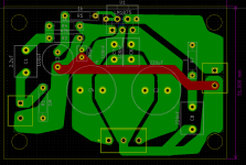
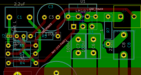
I moved all caps closer to the inputs of the IC and used pours to connect everything together. As a result of that, I was able to shrink PCB by almost 40%!The layout is decent, though you're not making very good use of the available copper. Also, I suggest moving the decoupling caps much closer to the IC. C6 and C7 should be right at the pins. C2 and C4 shouldn't be far away either. Right now, C2 and C4 are lined up with the IC, which means you'll have a hard time getting a screwdriver in to mount the IC. I suggest placing them closer to the IC and off to the right by enough that you can get a screwdriver in.
that looks like a good improvement.
that is something I never thought of before. I have the whole front surface available and I can just pour the ground onto it. But won't it mix current/voltage between signal ground between different points connected to that plane?I also suggest using a ground plane. You're paying for the copper anyway, so you might as well make it work for you.
After reading your articles on PCB layouts I decided to do a trick - put that resistor on the other side of the PCB connecting to the pins as close as possible. Would that be a good ides?The trace to R6 runs perilously close to the edge of the board. You want 50 mil (0.050" = 1.25 mm) minimum from the edge of the trace to the edge of the board. Otherwise, the trace might disappear when the board is cut from the panel.
That will require some tricky soldering, but hey, we're not doing mass-produce stuff in here, right?
Thank you for pointing out, I increased the width of signal traces to and replaced some tricky places with pours.You have a couple of acid traps in your layout (marked in red). You want to avoid traces coming together at acute angles as it can result in over-etching. It's not as big of an issue in the professional fabs as it used to be, but if you plan to etch the board yourself, you could end up with broken traces.
Is the PCB starting to look better?
Thanks to all one more time
Attachments
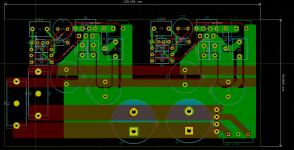
I keep going over Tom's articles and did quite a few changes to the schematic.
Firstly, decided to put a full stereo amp alongside the power supply on the same board. That will cut the costs of the fabrication process and costs on having less standoffs. A whopping $5.
Secondly, I separated all the different types of grounds along both channels of the amp folliwing Tom's approach.
So far it is looking good, I am proceeding to draft a 2 layer pcb. Will still try to keep the signal and power components separate. I also liked the idea of having a feedback resistor at the back of the PCB, I'll stick to that design.
Attachments
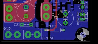
I am still a bit confused if I should be connecting C5 and C3 to the same ground.
Since C5 is the feedback cap, I'd expect it to be connected to the GND_LOAD, but it feels like C3 is acting as an input filter and should be connected to GND_SIG.
I would appreciate ideas on that matter.
Since C5 is the feedback cap, I'd expect it to be connected to the GND_LOAD, but it feels like C3 is acting as an input filter and should be connected to GND_SIG.
I would appreciate ideas on that matter.
The feedback capacitor is sampling the output, and referencing it to the input. Technically, it should be connected to a point between the two grounds (in terms of current flow). The input RF capacitor is always connected close to the chip input, which means a signal ground.
I find it easier to visualise ground as a connector with current flowing along it, rather than a series of points (even though a line is a series of points...). There are voltage drops along this line, and the feedback cap is bang in the middle.
However, it passes no current so if you separate grounds like you're doing with the 10 ohm resistor, it will connect to the lower noise side. Ideally the first thing after the breaking resistor, which by the way does not need to be larger than about 1 ohm to create the 'loop breaker' effect you're looking for.
I've attached a sample of how that should be done, though it's not the 1875.
Your second schematic makes more sense, including the way you've run the grounds.
Attachments
sangram, thank you for giving a hand with the input capacitors!
I decoupled C5's ground and now treat it as part of the signal ground. I am landing GND_SIG on the C3's pin that is connected to GND_LOAD.
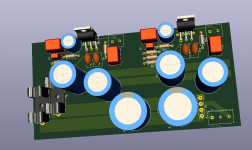
finished draft layout for the stereo PCB. nothing unusual in there, just 2 versions of the previous board side by side.
The boards are sparsely populated, so I used a fair bit of pours for ground, V+, and V-
Also, put in a couple of 4a fuses just in case.
I'll put more elbow grease into the layout tomorrow - the power rails for the decoupling capacitors may be done better and the fuses need to be repositioned.
All the signal traces are now 0,5 mm, wonder if I should try to make them 1 mm.
I repositioned the feedback caps closer to the input and tried to minimize all high voltage traces in the signal area.
The final PCB is still pretty small and will cost like $15 for 5.
I decoupled C5's ground and now treat it as part of the signal ground. I am landing GND_SIG on the C3's pin that is connected to GND_LOAD.
finished draft layout for the stereo PCB. nothing unusual in there, just 2 versions of the previous board side by side.
The boards are sparsely populated, so I used a fair bit of pours for ground, V+, and V-
Also, put in a couple of 4a fuses just in case.
I'll put more elbow grease into the layout tomorrow - the power rails for the decoupling capacitors may be done better and the fuses need to be repositioned.
All the signal traces are now 0,5 mm, wonder if I should try to make them 1 mm.
I repositioned the feedback caps closer to the input and tried to minimize all high voltage traces in the signal area.
The final PCB is still pretty small and will cost like $15 for 5.
Attachments
Put me down for a board if possible. I've got a couple of chips left.
will sure do!
just had a look at the tracking - will be arriving at my place any time this week
Code:
{"time":"2019/11/14 14:00:00","trackContent":"Released from customs: customs cleared."},
{"time":"2019/11/14 07:23:00","trackContent":"Shipment arrived at airport of destination country"},
{"time":"2019/11/13 19:00:00","trackContent":"shipment departed from airport of origin country"},Feedback please
Hi Guys,
Since this seems like an appropriate thread for such questions. Can I please get some feedback on an LM1875 board design.
I purchased some of the cheap ebay boards but after receiving them, I didn't like the look of them. They are too cramped and the pads are almost non existent.
I decided to make my own boards with the following goals:
1) Fuse clips back on the board like the old schoolies amp its derived from.
2) To allow for a 27.5mm pitch 22uF film cap for the feedback capacitor.
3) Input connection facing the back instead of the left side for ease of use.
4) Filter caps offset from the centreline of the LM1875 chip for ease of access with screw drivers.
5) Spade connections for output.
6) As small as possible.
I quickly figured out the spade connectors for power entry would take up less space as they can be tucked around the fuses unlike a 3pin screw terminal which is bulky.
I have 3 versions which I am wondering the merits of.
Here is the original pcb. 80mm by 63.5mm. I've managed to shave off a few mms despite the huge film cap.

1) Single layer PCB. It is based off the original schoolies pcb but optimised for the above design goals. I've preserved the separated ground sides.

2) 2 layer PCB. Preserves the layout of the single layer pcb but with all ground connections moved to the bottom and increased copper all around.


3) Solid ground 2 layer PCB. Ground plane pour over most of the pcb, the original separation of grounds completely gone. Maximised copper area.


Thoughts?
Hi Guys,
Since this seems like an appropriate thread for such questions. Can I please get some feedback on an LM1875 board design.
I purchased some of the cheap ebay boards but after receiving them, I didn't like the look of them. They are too cramped and the pads are almost non existent.
I decided to make my own boards with the following goals:
1) Fuse clips back on the board like the old schoolies amp its derived from.
2) To allow for a 27.5mm pitch 22uF film cap for the feedback capacitor.
3) Input connection facing the back instead of the left side for ease of use.
4) Filter caps offset from the centreline of the LM1875 chip for ease of access with screw drivers.
5) Spade connections for output.
6) As small as possible.
I quickly figured out the spade connectors for power entry would take up less space as they can be tucked around the fuses unlike a 3pin screw terminal which is bulky.
I have 3 versions which I am wondering the merits of.
Here is the original pcb. 80mm by 63.5mm. I've managed to shave off a few mms despite the huge film cap.
1) Single layer PCB. It is based off the original schoolies pcb but optimised for the above design goals. I've preserved the separated ground sides.
2) 2 layer PCB. Preserves the layout of the single layer pcb but with all ground connections moved to the bottom and increased copper all around.
3) Solid ground 2 layer PCB. Ground plane pour over most of the pcb, the original separation of grounds completely gone. Maximised copper area.
Thoughts?
Single layer has the advantage for tweaking and rework as 2 layer can be a pain for this. However, there may be (or not) advantages with the 2 layer for a set and forget.
It's a good idea to allow for different cap lead spacing as you have done on some but I'd also do that for the 470uF caps.
I can't see the 10R ground lift resistor but I suppose you decided to omit this.
It's a good idea to allow for different cap lead spacing as you have done on some but I'd also do that for the 470uF caps.
I can't see the 10R ground lift resistor but I suppose you decided to omit this.
Last edited:
iam not a PCB expert- but it looks improved.
i agree with rabbitz. try to get more solder spacing for the decoupling caps.
and
- C3 should be 100µF instead of 22µF - i see you have the space but the value is not correct.
- maybe for the 22k a parllel room for a small foil cap about 100pF/50V
chris
i agree with rabbitz. try to get more solder spacing for the decoupling caps.
and
- C3 should be 100µF instead of 22µF - i see you have the space but the value is not correct.
- maybe for the 22k a parllel room for a small foil cap about 100pF/50V
chris
Single layer has the advantage for tweaking and rework as 2 layer can be a pain for this. However, there may be (or not) advantages with the 2 layer for a set and forget.
It's a good idea to allow for different cap lead spacing as you have done on some but I'd also do that for the 470uF caps.
I can't see the 10R ground lift resistor but I suppose you decided to omit this.
Probably prudent really. I was planning to use some 10mm 470uf Panasonic FC caps I have on hand but a brief search on RS components suggests that 16mm diameter 7.5mm pitch is the more common size for 1000uF caps
I decided to remove the ground lift resistor as from what I have read around these forums it is probably unnecessary and doesnt feature on the spec sheet design.
iam not a PCB expert- but it looks improved.
i agree with rabbitz. try to get more solder spacing for the decoupling caps.
and
- C3 should be 100µF instead of 22µF - i see you have the space but the value is not correct.
- maybe for the 22k a parllel room for a small foil cap about 100pF/50V
chris
What would be the advantage of a 100uF cap instead of the 22uF? I am guessing the answer is a lower frequency rolloff?
Both the spec sheet and the schoolies design use 22uF.
The disadvantage would be cost. A 22uf film cap is around $7 on RS components however a 100uF film cap costs $25. This would necessitate going back to an elco cap. Which then begs the question as to whether a 100uF alco or a 22uF film cap would be superior.
Last edited:
- Status
- This old topic is closed. If you want to reopen this topic, contact a moderator using the "Report Post" button.
- Home
- Amplifiers
- Chip Amps
- Yet another LM1875 amp - review request