Hi everyone,
about 2 months ago I decided to take on the project of designing my own amplifier which is supposed to be driving my subwoofer in the future.
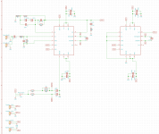
The circuit I chose to use is a dual TDA7293 parallel design.
I have attached my circuit diagram to this post. Please be aware, that I have already figured out and fixed the follow mistakes made:
- Capacitors C10 and C10P1 (1000u smoothing caps in negative supply rail) are polarized in the wrong direction, have turned them around on PCB
- Capacitor C3 polarized in wrong direction as well
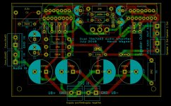
I have also attached an image of my PCB layout.
The power supply is a 24-0-24V toroidal transformer with a rectifier board attached to it (which did not have any problems and has worked perfectly fine from the beginning). It has 2 63V 10.000uF caps per rail.
Now the problems started when I first turned on my amplifier board.
On the first try I had both TDA7293 chips soldered to the board. I have shorted the audio input signal to ground.
In the instant I turned on power, both chipamps literally exploded, meaning they blew off part of the black cover of the IC.
Ofter the past weeks I quadruple checked again for mistakes in my layout and then soldered on a new TDA chip (this time only the one in the master position, because I had heard of the possibility of instability in parallel mode).
But the same thing happened again, instantly after powering on, a flame shoots out the bottom of the IC and that's it...
My last hope are now the great people in this forum who might be able to help me figuring out, what the problem with my amplifier design is.
I'm looking forward to your responses and suggestions and please don't hesitate to ask for any more info required to assess the situation.
about 2 months ago I decided to take on the project of designing my own amplifier which is supposed to be driving my subwoofer in the future.
The circuit I chose to use is a dual TDA7293 parallel design.
I have attached my circuit diagram to this post. Please be aware, that I have already figured out and fixed the follow mistakes made:
- Capacitors C10 and C10P1 (1000u smoothing caps in negative supply rail) are polarized in the wrong direction, have turned them around on PCB
- Capacitor C3 polarized in wrong direction as well
I have also attached an image of my PCB layout.
The power supply is a 24-0-24V toroidal transformer with a rectifier board attached to it (which did not have any problems and has worked perfectly fine from the beginning). It has 2 63V 10.000uF caps per rail.
Now the problems started when I first turned on my amplifier board.
On the first try I had both TDA7293 chips soldered to the board. I have shorted the audio input signal to ground.
In the instant I turned on power, both chipamps literally exploded, meaning they blew off part of the black cover of the IC.
Ofter the past weeks I quadruple checked again for mistakes in my layout and then soldered on a new TDA chip (this time only the one in the master position, because I had heard of the possibility of instability in parallel mode).
But the same thing happened again, instantly after powering on, a flame shoots out the bottom of the IC and that's it...
My last hope are now the great people in this forum who might be able to help me figuring out, what the problem with my amplifier design is.
I'm looking forward to your responses and suggestions and please don't hesitate to ask for any more info required to assess the situation.
Attachments
Are the TDA's screwed to a heat sink? Make sure they electrically isolated from the heat sink.
Your feedback is far too low, see the Ti specifications.
TDA7293 - 120 V / 100 W DMOS audio amplifier with mute and standby - STMicroelectronics
Your feedback is far too low, see the Ti specifications.
TDA7293 - 120 V / 100 W DMOS audio amplifier with mute and standby - STMicroelectronics
Use a bulb tester in the primary of your transformer (low wattage filament bulb, perhaps even a fridge type initially) and power up again with a new chip fitted and take some voltage checks. The bulb will prevent excess current and will light in the event of a fault.
In order to prevent excess current and possibly save the life of the next chipamp, this might be a solution, however, which voltages do you recommend checking?
Are the TDA's screwed to a heat sink? Make sure they electrically isolated from the heat sink.
Your feedback is far too low, see the Ti specifications.
TDA7293 - 120 V / 100 W DMOS audio amplifier with mute and standby - STMicroelectronics
I have not fitted a heat sink to the TDA's yet, since I wanted to first have my circuit work without any obvious problems in idle mode and then worry about heatsinking next.
Do you actually see any chance this might be a temperature problem? Because with the input signal shorted there should be barely any heat needing dissipation, right? Also, since the explosion occurs literally within less than one second after power up I wouldn't expect a heatsink to be having much of an effect on that?
Could you elaborate on the feedback being too low a bit more, please?
As I see it, my feedback is comprised of components R11/C3/C4/C5, in parallel with C6, in parallel with R5.
For a DC signal (f=0Hz), this should result in a resistance of 100kOhm (purely R5).
As the frequency of the signal rises, the impedance lowers. At a frequency of 20kHz, the impedance has dropped to roughly 19kOhms.
Are these calculations not correct? Are much higher frequencies to be observed in the feedback network?

In your layout, why does the negative supply go to the + side of the bypass caps and vice-versa?
This is one of the mistakes in my layout I mentioned in the first post. Capacitors C10 and C10P are polarized incorrectly and their orientation has been changed accordingly when assembling the PCB.
You should check all voltages to try and get a clue what is happening. Make sure the supply pins to the chip have the correct polarity of voltage, even if it limits out at a just a couple of volts with the bulb brightly lit. Does the output pin have voltage or does it seem stuck to zero volts (or a rail).
The TDA7293 ICs have the tendency to blow up if the negative rail disconnects for any reason or at any instant in time when the chip is powered up is not the most negative connection to the IC. Also, if you install the bootstrap capacitor backwards (eg polarity of cap is backwards) this can happen.
See if you can check for these problems in your amplifier.
There is more info on the web about these kind of issues with the TDA7293 if you search for it.
See if you can check for these problems in your amplifier.
There is more info on the web about these kind of issues with the TDA7293 if you search for it.
Hi Marco,
You write: "...a dual TDA7293 parallel design...". Though it is difficult for me to see all details of the PCB layout, I get the impression that you indeed have connected the outputs in parallel without cross conduction limiting resistors? If so, you have a major problem here.
You write: "...with the input signal shorted there should be barely any heat needing dissipation, right?" In theory right but not if you have amplifier self-oscillation".
Either C3 or C4 have to be turned around if you try to make a bipolar capacitor. Add two 1N4148 diodes in parallel for voltage control.
Last edited:
TDA7293 doesn't need resistors at the outputs. I don't think that there are any errors in the schematic. The PCB is not so great (really bad). Why didn't you just copy the layout from the datasheet?
Remove the TDA and measure the resistance between input, output, power and ground. If the power sequence is not correct the chip will explode. Connect + 0 - and check the voltages at the power pins. Also, check if the mute/stby circuits work. If the mute/stby is not correct the chip will explode. Only then install the TDA. You will need some kind of heatsink attached to the chip for it to work correctly. Without the heatsink, the chip will explode.
Remove the TDA and measure the resistance between input, output, power and ground. If the power sequence is not correct the chip will explode. Connect + 0 - and check the voltages at the power pins. Also, check if the mute/stby circuits work. If the mute/stby is not correct the chip will explode. Only then install the TDA. You will need some kind of heatsink attached to the chip for it to work correctly. Without the heatsink, the chip will explode.
Last edited:
TDA7293 doesn't need resistors at the outputs. I don't think that there are any errors in the schematic. The PCB is not so great (really bad). Why didn't you just copy the layout from the datasheet?
Remove the TDA and measure the resistance between input, output, power and ground. Connect + 0 - and check the voltages at the power pins. Also, check if the mute/stby circuits work. Only then install the TDA. You will need some kind of heatsink attached to the chip for it to work correctly.
Mark, my point is that two TDA7293 seem to have been put in parallel at the outputs simply by a direct connection between them. Pin 14 of the first TDA7293 seems connected to pin 14 of the second TDA7293. Could it arise from the use of terminal "SPK+" at both outputs?
Last edited:
To begin with, your schematic is wrong. It will never work as is.
1) you only show the left amp connected to signal, ground, supply rails, NFB and speaker.
the right one has the following gross errors, I am very surprised nobody pointed at them:
a) the right amp has no signal feeding it.
b) +I, -IN and Signal Gnd are not only shorted among them but ... directly connected to -Vb!!!!
That alone will destroy the right side chipamp.
c) its output is directly connected to the left amp output, so it will carry it to its grave too.
d) plus somewhat smaller errors such as unconnected Stby and Mute, etc.
Side comment: why worry about stability, heatsinking, light bulb limiters, etc. etc. when these errors will NUKE the amp.
Yes Mark, you are the only one who knows how to read here.FauxFrench, isn't that the way it has been done in the datasheet, figure 11, where one is placed in slave mode?
Am I the only one who reads datasheets?
You are right, Fig.11 shows that "Modular application" can use the outputs connected in parallel, directly.
As you are the only one to read here, would you know which is the "slave IN pin" described as "The slave IN pin must be connected to the negative supply" (section 4.4, last bullet)?
As an illiterate, I find it likely that the second TDA7293 is actually not acting correctly as a slave and thereby loads the output of the first TDA7293.
To begin with, your schematic is wrong. It will never work as is.
1) you only show the left amp connected to signal, ground, supply rails, NFB and speaker.
the right one has the following gross errors, I am very surprised nobody pointed at them:
a) the right amp has no signal feeding it.
b) +I, -IN and Signal Gnd are not only shorted among them but ... directly connected to -Vb!!!!
That alone will destroy the right side chipamp.
c) its output is directly connected to the left amp output, so it will carry it to its grave too.
d) plus somewhat smaller errors such as unconnected Stby and Mute, etc.
Side comment: why worry about stability, heatsinking, light bulb limiters, etc. etc. when these errors will NUKE the amp.
When paralleling these, the second chip only has its output stage in use.
Pin 11 (Buffer Driver) operates as an output pin in the first chip. Pin 11 in the slave chip is an input and selected by connecting the - and + inputs to the negative rail.
Direct connection of the two outputs is permitted.
Standby and mute are in parallel for the two chips.
That all seems OK in the diagram in post #1 as far as I can see.
Thanks guys for all your input.
I have read about the issue of the chip exploding when the negative supply rail disconnects, am wondering how this would be possible though. Both fuses, in the negative supply as well as the positive one stayed intact so it seems unlikely that one of the rails disconnected.
I will however desolder the single blown chip now and power the circuit up without it to check for correct voltages on all PCB pads!
The bootstrap capacitor is in my schematic oriented the same way as in the modular application figure in the TDA data sheet if I am not mistaken, so this should not be the issue.
Is my layout really that different from the data sheet? In what aspects is it really bad? I am very interested in that so I can learn for my future designs.
I will measure these resistances. What values should I expect there?
I have found one very interesting thing concerning resistances: Before powering up my circuit, I actually did check the resistances between ground and the two power rails and found I relatively high resistance of about 300-400kOhm between ground and the positive supply, but a very low resistance of only 35 Ohms between ground and the negative rail. First I thought this might be a mistake in my circuit but then I measured the same resistances directly at the pins of a not-soldered TDA7293 and found the same values.
Why is the resistance between signal ground and the negative so much lower with this chip???
I believe you are not correct with your assumptions. The second amp is configured for slave mode with it's Input, Feedback and signal Ground connected to the negative supply rail. This is shown in the modular application according to the TDA7293 data sheet.
The "slave IN" pin as I see it is simply the input pin of the second TDA chip which gets shorted to its feedback pin and the negativ supply instead of feeding it an audio signal.
As I wrote in my opening post this was exactly my thought and I did as you described. Only on my very first power-up and explosion were both chips soldered to the board. For my second attempt I only soldered in said master chip but experienced exactly the same destructive behavior.
You should check all voltages to try and get a clue what is happening. Make sure the supply pins to the chip have the correct polarity of voltage, even if it limits out at a just a couple of volts with the bulb brightly lit. Does the output pin have voltage or does it seem stuck to zero volts (or a rail).
The TDA7293 ICs have the tendency to blow up if the negative rail disconnects for any reason or at any instant in time when the chip is powered up is not the most negative connection to the IC. Also, if you install the bootstrap capacitor backwards (eg polarity of cap is backwards) this can happen.
See if you can check for these problems in your amplifier.
There is more info on the web about these kind of issues with the TDA7293 if you search for it.
I have read about the issue of the chip exploding when the negative supply rail disconnects, am wondering how this would be possible though. Both fuses, in the negative supply as well as the positive one stayed intact so it seems unlikely that one of the rails disconnected.
I will however desolder the single blown chip now and power the circuit up without it to check for correct voltages on all PCB pads!
The bootstrap capacitor is in my schematic oriented the same way as in the modular application figure in the TDA data sheet if I am not mistaken, so this should not be the issue.
TDA7293 doesn't need resistors at the outputs. I don't think that there are any errors in the schematic. The PCB is not so great (really bad). Why didn't you just copy the layout from the datasheet?
Remove the TDA and measure the resistance between input, output, power and ground. If the power sequence is not correct the chip will explode. Connect + 0 - and check the voltages at the power pins. Also, check if the mute/stby circuits work. If the mute/stby is not correct the chip will explode. Only then install the TDA. You will need some kind of heatsink attached to the chip for it to work correctly. Without the heatsink, the chip will explode.
Is my layout really that different from the data sheet? In what aspects is it really bad? I am very interested in that so I can learn for my future designs.
I will measure these resistances. What values should I expect there?
I have found one very interesting thing concerning resistances: Before powering up my circuit, I actually did check the resistances between ground and the two power rails and found I relatively high resistance of about 300-400kOhm between ground and the positive supply, but a very low resistance of only 35 Ohms between ground and the negative rail. First I thought this might be a mistake in my circuit but then I measured the same resistances directly at the pins of a not-soldered TDA7293 and found the same values.
Why is the resistance between signal ground and the negative so much lower with this chip???
To begin with, your schematic is wrong. It will never work as is.
1) you only show the left amp connected to signal, ground, supply rails, NFB and speaker.
the right one has the following gross errors, I am very surprised nobody pointed at them:
a) the right amp has no signal feeding it.
b) +I, -IN and Signal Gnd are not only shorted among them but ... directly connected to -Vb!!!!
That alone will destroy the right side chipamp.
c) its output is directly connected to the left amp output, so it will carry it to its grave too.
d) plus somewhat smaller errors such as unconnected Stby and Mute, etc.
Side comment: why worry about stability, heatsinking, light bulb limiters, etc. etc. when these errors will NUKE the amp.
I believe you are not correct with your assumptions. The second amp is configured for slave mode with it's Input, Feedback and signal Ground connected to the negative supply rail. This is shown in the modular application according to the TDA7293 data sheet.
Yes Mark, you are the only one who knows how to read here.
You are right, Fig.11 shows that "Modular application" can use the outputs connected in parallel, directly.
As you are the only one to read here, would you know which is the "slave IN pin" described as "The slave IN pin must be connected to the negative supply" (section 4.4, last bullet)?
As an illiterate, I find it likely that the second TDA7293 is actually not acting correctly as a slave and thereby loads the output of the first TDA7293.
The "slave IN" pin as I see it is simply the input pin of the second TDA chip which gets shorted to its feedback pin and the negativ supply instead of feeding it an audio signal.
Marco, would it be possible that you test the first TDA7293 (master) before putting the second TDA7293 (slave) in? If the master TDA7293 can function on its own, it is likely that it is loaded by the second TDA7293.
As I wrote in my opening post this was exactly my thought and I did as you described. Only on my very first power-up and explosion were both chips soldered to the board. For my second attempt I only soldered in said master chip but experienced exactly the same destructive behavior.
A thought: if the -supply is disconnected, how can it then blow up? Where is that 'blow up current' going to/coming from? Whats the path? Presumably from +supply but where to? Is there a ground connection at the chip, except for the standby pin?
Are we sure there are no other errors??
Edit: I see JMFahey has already pointed them out. Problem identified and diagnosed.
Jan
Are we sure there are no other errors??
Edit: I see JMFahey has already pointed them out. Problem identified and diagnosed.
Jan
Last edited:
47µF would be the vaule for the bootstrap cap if it's shared. It's not clear what happens if the slave has its own bootstrap feedback, but if it does it should probably be the nominal 22µF. I'd just connect it to the master like in the datasheet, there could be something special about that since the inputs on the slave are connected to the negative rail and effectively unused. So who knows.
Is my layout really that different from the datasheet? In what aspects is it really bad? I am very interested in that so I can learn for my future designs.
Optimizing TDA7294 Output
A link to some just for fun layouts that I made for a TDA7293/4 S/V board. Wide power traces. Input ground and feedback connect together then connect to the speaker return (R6 middle of the board).
danielwritesbac is the expert on these chips. I planned to build both but didn't like the reliability problems.
Last edited:
You definitely need a heat sink.
Your circuit doesn't look right to me.
Its very different to a TDA7294 circuit which is pretty much the same chip.
Gain should be at least 20 or the device will oscillate.
Feedback resistor path should be as short as possible.
I recently built up a tda7294 hybrid valve/chip amp circuit.
The fuses blew straight away.
When I investigated it there was a short directly across b+ and b-.
The only place I could see a possible short was on the chip legs for the b+/b- against the pcb.
After I removed the tda the short went away.
So I bought in a new tda and soldered it in but this time a couple of mm off the pcb.
This time it worked fine.
Last edited:
- Home
- Amplifiers
- Chip Amps
- TDA7293 Amplifier Design Blows Up Instantly