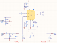
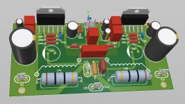
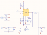
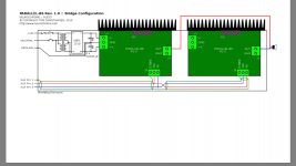
Howdy all! Right, after a couple of successful hard-wired, kit and breadboard LM3886 builds I'm starting to put together the LM3886 boards as detailed here. Essentially, 2 DRV134s driving 4 sets of paralleled LM3886es. So 8 LM3886es in total for the stereo amp.
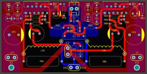
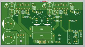
Attached is my first stab at the parallel PCB. This is inspired by a bunch of different PA100 builds from in and around the internet, as well as @tomchr's Taming the LM3886 pages for component values.
Notes:
At this point, I think the bottom layer is working pretty well, but the top layer seems needlessly complex. My temptation is to just flood it with a ground pour, minus the cross-shaped input ground.
Any comments/feedback/suggestions/advice for a fellow traveler?")
Attached is my first stab at the parallel PCB. This is inspired by a bunch of different PA100 builds from in and around the internet, as well as @tomchr's Taming the LM3886 pages for component values.
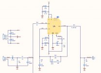
- The schematic shows only one of the parallel pairs - the second LM3886 is identical, replace the "A"s in the designators for "Bs".
- Power (as per @tomchr's recommendation) will be +/-28V
- I've thumbsucked the dimensions of my inductors - LA1 and LB1 - I'll be winding some today, but I doubt the dimensions will be far off.
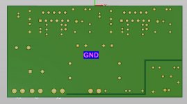
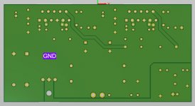
Notes:
- Top (red) pours: The two red planes are GND pours, separating the two chips and meeting at the GND spade terminal (X2).
- Top (red) traces: These are the majority of the signal tracks. In addition, CA7 and CB7 get their own GND traces back to the X2 GND terminal.
- Bottom (blue) pours: 3 planes, for V+ along the left, V- along the right and a cross-shaped GND plane for the input and output grounds, meeting at a small star point between C2 and R2
- Bottom (red) traces: Only a few traces here for the output (X5).
At this point, I think the bottom layer is working pretty well, but the top layer seems needlessly complex. My temptation is to just flood it with a ground pour, minus the cross-shaped input ground.
Any comments/feedback/suggestions/advice for a fellow traveler?
Attachments
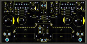
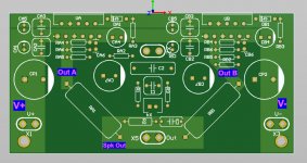
Many layouts wind the output inductors around the output resistors - that might give you a little more space here (especially if you position the resistors at an angle)?
Just looking at the layout I don't understand why the CAx and CBx caps aren't oriented the same way between the two halves of the board. Admittedly it probably doesn't matter much, but it triggers my OCD a bit
Also you might be able to shorten a couple of traces here and there by:
- turning CA7 and CB7 90 degrees (or even CA7 180 degrees)
- turning R1, R3 and C1 90 degrees
- swapping Rx4 and Rx6 around (possibly)
Many layouts wind the output inductors around the output resistors - that might give you a little more space here (especially if you position the resistors at an angle)?
Ooh, interesting - will see if this can be done!
Just looking at the layout I don't understand why the CAx and CBx caps aren't oriented the same way between the two halves of the board. Admittedly it probably doesn't matter much, but it triggers my OCD a bit
Ha ha, fair enough - will see what I can do
Also you might be able to shorten a couple of traces here and there by:
- turning CA7 and CB7 90 degrees (or even CA7 180 degrees)
- turning R1, R3 and C1 90 degrees
- swapping Rx4 and Rx6 around (possibly)
Well spotted. Done!
Thanks very much!
I suggest reading Douglas Self's amplifier design book - or his article series from Wireless World published in the mid 1990ies, which formed the basis for the book. Your supply routing is about the worst you can do for rail-induced distortion.
Your VEE connection is super skinny. You'll be pushing 7A+ through that...
The curved traces do nothing for you and in one case, you've created an acid trap (T intersection under R1).
You'll need ballast resistors as well.
Tom
Your VEE connection is super skinny. You'll be pushing 7A+ through that...
The curved traces do nothing for you and in one case, you've created an acid trap (T intersection under R1).
You'll need ballast resistors as well.
Tom
Thanks for the feedback everyone!
Yeah, in the interests of saving space on the board I'm tempted to do the @AndrewT approach of putting the R/L's at the speaker terminals, off-board.
...which means I'll also have room for the 1% output resistors! Thanks!
Agreed - the fattening shall begin! @tomchr raises serious concerns about my grounding layout (as suspected) so I'll redo that and then see how best to fatten up the output.
Thanks for the suggestion! I read the one on Small Signals, will try grab a copy of the Power Amplifier Design book.
Ha ha, I appreciate the brutal honesty. I have a lot to learn!
Would it be worthwhile running say, V+ on the top and V- on the bottom? That way, they won't be competing for space to the LM3886 ICs, and can be as fat as needed? The centre of the PCB could then be used on both top and bottom for various grounds.
Gotcha!
I would not use a pair of R/L for each chip, just one for both, or for all of the chips.
I would add 1% 0.1-0.3ohms/3-5 watts output resistor for each chip .
Servo is optional.
Yeah, in the interests of saving space on the board I'm tempted to do the @AndrewT approach of putting the R/L's at the speaker terminals, off-board.
...which means I'll also have room for the 1% output resistors! Thanks!
If your "out" trace is just the thin blue one, then it should probably be made thicker (looks like there is space for that).
Agreed - the fattening shall begin! @tomchr raises serious concerns about my grounding layout (as suspected) so I'll redo that and then see how best to fatten up the output.
I suggest reading Douglas Self's amplifier design book - or his article series from Wireless World published in the mid 1990ies, which formed the basis for the book.
Thanks for the suggestion! I read the one on Small Signals, will try grab a copy of the Power Amplifier Design book.
Your supply routing is about the worst you can do for rail-induced distortion.
Ha ha, I appreciate the brutal honesty. I have a lot to learn!
Your VEE connection is super skinny. You'll be pushing 7A+ through that...
Would it be worthwhile running say, V+ on the top and V- on the bottom? That way, they won't be competing for space to the LM3886 ICs, and can be as fat as needed? The centre of the PCB could then be used on both top and bottom for various grounds.
You'll need ballast resistors as well.
Gotcha!
To give you an idea: PCB for paralleled inverting lm3886, with buffer and servo
Not perfect by a long shot but that's the overall direction wrt PS and ground. Read Tom's comments at the end of the thread.
Not perfect by a long shot but that's the overall direction wrt PS and ground. Read Tom's comments at the end of the thread.
Thanks @00940 - great reference.
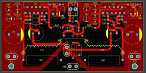
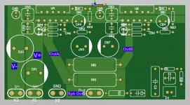
Okay, I'm starting from scratch. Before I get too carried away, I just wanted to get an opinion on the following pour layout, using suggestions above. The power pours are now much larger and consistent in thickness, the outputs are now chunky instead of individual traces. The entire ground plane (on the bottom) has been flooded, with some separation near the input section as per @tomchr's feedback in this thread.
I've not routed anything else except for the two output traces from the LM3886es to the output pours - attached are just the pours as a work in progress, the text/component placement is still a little messy. But does this look good from a general grounding and pour perspective?
Attachments
Last edited:
I see that you insist in having v+ in one side and v- in the other side of the board, that means you'll have unnecessary longer cables from the power supply to the amplifier board , and I think would not look so neat. Am I the only one who's not a big fan of diagonal components?
You might have a look at this too: DIY BPA300 6x LM3886 300W audio Amplifier
Looks much better, I can't see how pins no 3 for the ic s are connected.I would connect them to ra6/ra4 on the bottom of the board so you can leave V+ Copper pour as wide is possible.
As mentioned the example images are pretty much just the pours for now, but will keep this in mind. Thanks for the feedback! Will forge ahead with this general layout.
The output ground is missing in both the schematic and PCB.
@Mark - this is intended for use in a balanced/parallel setup - another identical board is handling (what would be) the output ground - see here.
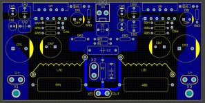
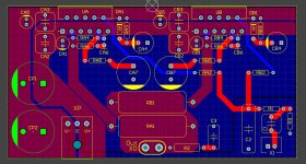
Okay, what I'm calling version "4", attached.
Lots has changed, used the ground layout settled on with @asuslover - I'm preferring the grouping of the power pins as well, which has been consolidated into a fat Molex style power connector.
Ballast resistors (0.1R) added as well.
Most of the heavy-duty connections are now handled by pours, with a few traces on the top (and a couple on the bottom) handling signal paths.
Things to do: add an output ground, add mounting holes.
Is this looking any better? Worse? Hit me
Attachments
Those halves of your amp should be working individually , I would focus on designing an fully working amp (output ground is a must) and then bridge 2 of them.
This is how Tom is suggesting this to be done.
Beat me to it! This is on the to-do list for v5
Thanks!- Status
- This old topic is closed. If you want to reopen this topic, contact a moderator using the "Report Post" button.
- Home
- Amplifiers
- Chip Amps
- Critique my PCB! Yet another parallel LM3886