I built it for a friend 18 months ago, I think it is excellent.Has anyone built this amp.
I have the Gerber files available on my hobby website (with links to this page) and they have been accessed over 1000 times, so I would say there are probably a fair few completed amps out there. Very few people come to this page asking for help which could suggest they haven't had any real problems with it.
It's relatively cheap to build, why not just send the files off and give it a go?
Thanks for confirming the drill size. My digital calipers aren't good enough (and probably aren't the right tool) to check them since I get a reading of 1.2x mm.AWG18 should fit without problem, AWG16 will be too tight. The drill hole is a 1.3mm one.
I was considering whether to solder wires directly to the board or use a terminal block. At the end of the day I suppose anything other than soldering (at least for my application) would just be a waste of time and money, as 18 AWG is more than enough for how much power I need out of these.
Has anyone built this amp.
I built one for my summer house, sounds great
") recommended
recommended 
for the DC protect: https://www.diyaudio.com/forums/chip-amps/321922-source-layout-lm3886-13.html#post5606986
for the PSU: ok, a bom was here: An open source layout for LM3886? but it's not fully correct. Caps and resistors should be fine but the final version uses the bridges mentioned in post 63. The heatsink should rather be the Ohmite RA-T2X-38E
for the PSU: ok, a bom was here: An open source layout for LM3886? but it's not fully correct. Caps and resistors should be fine but the final version uses the bridges mentioned in post 63. The heatsink should rather be the Ohmite RA-T2X-38E
Last edited:
Has anyone built this amp.
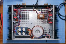
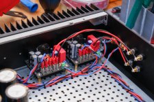
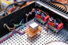
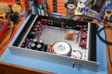
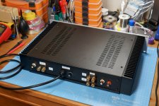
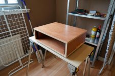
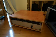
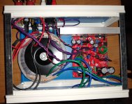
I just realised I only posted my build to the main gallery thread & never actually contributed back to this thread. I finally finished it back in May this year, after starting in 2018.
It is a 3 channel build for a 2.1 setup, with two of the boards bridged via a Vigortronix VTX-101-007 audio transformer. There is a lot of empty space in the enclosure because I originally intended to house an active crossover & its power supply in the same enclosure, but in the end I stuck with my separate dbx crossover. I know my hand wound coils are bad, but I have to leave myself something to improve on next time.
I also built a 3U rack from some cheap plywood.
I am very happy with the results. I used my last gainclone for 8+ years & I now intend to use this one for 8+ more.
Attachments
Last edited:
Are these files good to go to the forge?
First of all, many thanks... I've been looking for a project like this for so long...
I'm planning on printing the PCB's and make (another) an amp for myself
So... I have some questions:
Are these gerber the final version? Anything I should be worried about? Do you have a BOM's list? (found them, thanks)I don't want to mess it up
And thank you so much for all that work, it looks amazing by the way
Well, there are two issues here. One is how things are joined and the impact of common tracks' impedance. No objection on that, the feedback cap has to go to the input gndplane. The other thing, less clear, is about loop area and radiations pickup. Groundplanes are relevant to both issues as provide a low impedance connection but also allow to reduce some loops.
So, here's an attempt to satisfy all the compromises. Yeah, I wish... As before, the zip is for the eagle files.
The feedback cap now returns to the input gnd. The feedback resistor going to gnd is over the split between the signal and the power gndplanes. If you consider the loop mentioned in the post above, it's quite tight.
The two gndplanes are joined near the output connectors by a resistor. It can be jumpered in case of a mono amp.
Better now ?
First of all, many thanks... I've been looking for a project like this for so long...
I'm planning on printing the PCB's and make (another) an amp for myself
So... I have some questions:
Are these gerber the final version? Anything I should be worried about? Do you have a BOM's list? (found them, thanks)I don't want to mess it up
And thank you so much for all that work, it looks amazing by the way
Last edited:
That is exactly how this chipamp mania started.
View attachment 677920
WTF is that?
When the files are uploaded to JLCPCB, only the amp board autofills in the dimensions of the board and allows previewing of the PCB.
The Power supply board and Protect board do not auto fill the board size and you cannot preview the PCB with their online Gerber viewer.
Any ideas why?
The Power supply board and Protect board do not auto fill the board size and you cannot preview the PCB with their online Gerber viewer.
Any ideas why?
You have to search for Gaincard. Very interesting product and design style.WTF is that?
It might very well be that I messed up and never uploaded the gerbers but only the Eagle filesThe Power supply board and Protect board do not auto fill the board size and you cannot preview the PCB with their online Gerber viewer.
Any ideas why?

They haven't been very popular to start with so it's never been pointed out. I'll reinstall Eagle and generate gerbers.
My apologies
Gerbers
Thanks for this project, it looks like just what I've been looking for!
What version of Eagle are you running?
I tried to open the files, but my (quite old and in need of update) version of Eagle errored on them.
When you get a chance to do the PS and protection gerbers, it would be nice to have them.
Many thanks!
Adam
I re-attached all the files to this post.
The files open without problem with Eagle 8.7.1
The files open without problem with Eagle 8.7.1
Attachments
I just want to thank you for making this design public and available for everyone. This is really helpful to me as someone who is just getting into playing around with chipamps, and I think the difference between 0.001% and 0.000000001% THD is mostly academic and completely inaudible to human ears. So this amp design more than delivers on performance as compared to some of the other, composite LM3886 designs I've seen on this forum. Thank you so much for this design!
Changing Gain
Hi Guys,
A quick question.
I am about to build another pair of these but I want much lower gain this time round. Something like a gain of 13.
R5 is easy, I would simply change to 12k.
However I am uncertain what to do with the filter of R7 and C5.
Do I need to change R7 from 22k to 12k as well?
Hi Guys,
A quick question.
I am about to build another pair of these but I want much lower gain this time round. Something like a gain of 13.
R5 is easy, I would simply change to 12k.
However I am uncertain what to do with the filter of R7 and C5.
Do I need to change R7 from 22k to 12k as well?
The Power supply board and Protect board do not auto fill the board size and you cannot preview the PCB with their online Gerber viewer.
Any ideas why?
That sort of stuff often happens if the FAB layer is missing. The FABrication drawing is basically the board outline and through-hole locations.
For a two-layer board with top silk screen, you need the following files:
- Top copper
- Bottom copper
- Top solder mask
- Bottom solder mask
- Top silk screen
- Echelon (X,Y) file for the through-holes
- Fabrication drawing
Your layout tool should be able to produce these in Gerber 2.74 format.
Tom
Last edited:
I just finished my version of the Super Gain Clone stereo amp board. It places the rectifier and two channels on a single PCB.
GitHub - profdc9/SuperGainClone: A stereo layout of Bob Cordell's Super Gain Clone amplifier.
You can download the whole project, kicad, gerbers, and all using the Download button. I have a picture of my build below.
GitHub - profdc9/SuperGainClone: A stereo layout of Bob Cordell's Super Gain Clone amplifier.
You can download the whole project, kicad, gerbers, and all using the Download button. I have a picture of my build below.
Attachments
- Home
- Amplifiers
- Chip Amps
- An open source layout for LM3886?