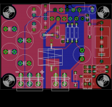
Remove the PGND plane from under the input and feedback traces/parts. The AGND plane goes under the input and feedback circuits only.
Add the option of a Hum Breaking Resistor between the output GND and AGND. This will
help when you use multiple boards connected to a single transformer.
The LM3886 inputs are high impedance, keeping these traces short will prevent hum.
a quick explanation of the reasoning behind this helps others learn the practical tricks, pitfalls behind layouts. I mean from the perspective of inexperienced designers. There are many books explaining the art, but nothing like practical tit-bits from experienced folks.
thanks
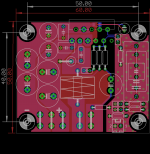
Trying to address a few suggestions.
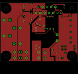
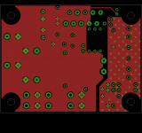
- the feedback cap is now clearing the way to the lm3886 screw")
- the rf input filter is now ahead of the input cap. It's creating a voltage divider with the input resistor but the signal loss isn't big. The input tracks are significantly shorter. Most of the input tracks are under the signal ground plane only.
- there is now a resistor between signal gnd and power gnd. Easily jumpered if not needed.
I'm yet to be convinced of the need to clear the power gndplane near the lm3886 input pins...
- the feedback cap is now clearing the way to the lm3886 screw
- the rf input filter is now ahead of the input cap. It's creating a voltage divider with the input resistor but the signal loss isn't big. The input tracks are significantly shorter. Most of the input tracks are under the signal ground plane only.
- there is now a resistor between signal gnd and power gnd. Easily jumpered if not needed.
I'm yet to be convinced of the need to clear the power gndplane near the lm3886 input pins...
Attachments
Most of the reasoning can be found in the datasheet.
LAYOUT, GROUND LOOPS AND STABILITY
The LM3886 is designed to be stable when operated at a closed-loop gain of 10 or greater, but as with any other high-current amplifier, the LM3886 can be made to oscillate under certain conditions. These usually involve printed circuit board layout or output/input coupling.
When designing a layout, it is important to return the load ground, the output compensation ground, and the low level (feedback and input) grounds to the circuit board common ground point through separate paths. Otherwise, large currents flowing along a ground conductor will generate voltages on the conductor which can effectively act as signals at the input, resulting in high frequency oscillation or excessive distortion. It is advisable to keep the output compensation components and the 0.1 μF supply decoupling capacitors as close as possible to the LM3886 to reduce the effects of PCB trace resistance and inductance. For the same reason, the ground return paths should be as short as possible. In general, with fast, high-current circuitry, all sorts of problems can arise from improper grounding which again can be avoided by returning all grounds separately to a common point. Without isolating the ground signals and returning the grounds to a common point, ground loops may occur. “Ground Loop” is the term used to describe situations occurring in ground systems where a difference in potential exists between two ground points. Ideally a ground is a ground, but unfortunately, in order for this to be true, ground conductors with zero resistance are necessary. Since real world ground leads possess finite resistance, currents running through them will cause finite voltage drops to exist. If two ground return lines tie into the same path at different points there will be a voltage drop between them. The first figure below shows a common ground example where the positive input ground and the load ground are returned to the supply ground point via the same wire. The addition of the finite wire resistance, R2, results in a voltage difference between the two points.
The single-point ground concept should be applied rigorously to all components and all circuits when possible. Violations of single-point grounding are most common among printed circuit board designs, since the circuit is surrounded by large ground areas which invite the temptation to run a device to the closest ground spot. As a final rule, make all ground returns low resistance and low inductance by using large wire and wide traces. Occasionally, current in the output leads (which function as antennas) can be coupled through the air to the amplifier input, resulting in high-frequency oscillation. This normally happens when the source impedance is high or the input leads are long. The problem can be eliminated by placing a small capacitor, CC, (on the order of 50 pF to 500 pF) across the LM3886 input terminals. Refer to External Components Description relating to component interaction with Cf.
Most of the reasoning can be found in the datasheet.
Cf.
I found the feedback resistor path needs to be as short as possible.
As for minimum gain you can get around it by putting 100pf between + and - inputs. I fell foul of that in a TDA7294 design that had a valve pre amp and I had reduced the gain to around 8. The cap stopped it oscillating.
Mark: all of those points raised by the datasheet are addressed by the current layout.
I'd be more interested to know why you are concerned by the power groundplane under the feedback network.
Current in the output leads (which function as antennas) can be coupled through the air to the amplifier input, resulting in high-frequency oscillation.
The power ground plane carries high current. Why would you want to place it under the feedback and/or input circuits?
I found the feedback resistor path needs to be as short as possible.
As for minimum gain you can get around it by putting 100pf between + and - inputs. I fell foul of that in a TDA7294 design that had a valve pre amp and I had reduced the gain to around 8. The cap stopped it oscillating.
Ben already covered the rationale of tapping the Rf between -in and the edge of the Zobel. Likewise, the other compensation networks are in place.
@Mark: My antenna theory is rusty but the problem isn't having the power groundplane under the signal tracks. It is more about the couple power tracks-groundplane and how it radiates. Untwisted output leads are way more problematic than having power lines over a continuous groundplane.
Furthermore, at the highish frequencies threatening oscillation, there will be less current flowing in the plane under the feedback network. Current will gather more under the output tracks as frequency goes up.
Anyway, I can check again my smd layout for oscillation. It's even more compact and "worse" under that respect.
Most of the reasoning can be found in the datasheet.
LAYOUT, GROUND LOOPS AND STABILITY........
.
Thanks
The only reason I would be worried about the ground plane under the the FB network is parasitic capacitance. How major that is vs having something like a 9k (at G=10, where this circuit is probably most relevant!) feedback resistor, I'm not sure. We're not talking a high-speed opamp or anything, and the better the ground plane, the less voltage drop there is across it.
On my TDA7294 layout I put a copper pour connected to zero volts under most of the circuit.
I deliberately left out Zobel ground path and power supply ground path to a star ground point. Then connected copper pour to ground at star ground point.
Sounded great with no hum or noise.
Its important b+ and b- come into smoothing caps first then go on to TDA7294.
Possibly the most important point is the feedback resistor path should be as short as possible or you can get oscillation.

@dazcwl: see http://www.diyaudio.com/forums/chip-amps/295665-neurochrome-lm3886dr-build-3.html#post4815099
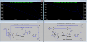
See the attached sim. Blue/green are the output of the left (ideal) and middle circuit ("bad layout" with output inductor). Red is the circuit at the right ("bad layout" without output inductor). It confirms Tom's post. After all, there are plenty of very good amps with longish feedback resistor path (slewmaster, astx EF2 among others).
@DPH: yes, capacitive coupling isn't a big concern here I'd think. I borrowed Ott's "Noise Reduction Techniques in Electronic Systems" from my brother, going to go through it, the first chapters seem useful.
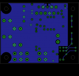
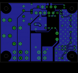
Still, here's a 'hardened' version. I moved the power groundplane to the top layer. The area around the input pins is emptied.
See the attached sim. Blue/green are the output of the left (ideal) and middle circuit ("bad layout" with output inductor). Red is the circuit at the right ("bad layout" without output inductor). It confirms Tom's post. After all, there are plenty of very good amps with longish feedback resistor path (slewmaster, astx EF2 among others).
@DPH: yes, capacitive coupling isn't a big concern here I'd think. I borrowed Ott's "Noise Reduction Techniques in Electronic Systems" from my brother, going to go through it, the first chapters seem useful.
Still, here's a 'hardened' version. I moved the power groundplane to the top layer. The area around the input pins is emptied.
Attachments
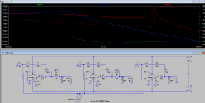
Yes, the quick sim above isn't conclusive about stability (and the lm3886 ltspice model is uncertain anyway). Still, the presence or absence of peaking shows that the output inductor indeed positively impacts the stability in the presence of parasitic inductance in the tracks, as you mentioned.
Here is a better sim, using the Tian probe, showing the same.
edit: oh, and Ott's book mentioned above is great
Here is a better sim, using the Tian probe, showing the same.
edit: oh, and Ott's book mentioned above is great
Attachments
Last edited:
Considering the thread is going silent, the pcb must be kind of fine as is.
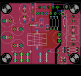
I went through Mouser to create a BOM. Total cost to populate a pcb with decent parts (wima, vishay, nichicon, panasonic, tdk and the like) is 19.50€ (before VAT).
Time to layout a companion power supply board.
I went through Mouser to create a BOM. Total cost to populate a pcb with decent parts (wima, vishay, nichicon, panasonic, tdk and the like) is 19.50€ (before VAT).
Time to layout a companion power supply board.
Attachments
- Home
- Amplifiers
- Chip Amps
- An open source layout for LM3886?