After building the BA100 with P2p a few years ago, I'm trying to challenge myself to build the BPA200. I am planing to use the diagram from the AN-1192 document. I have a few questions that I will list below:
1) I am planing to do P2p for BPA200 as well, any drawbacks to this? (considering the extra opamp stages, I'm wondering if this circuit is more prone to stray noise or inductance introduced by long traces or p2p connections)
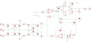
2) Are there any further modifications recommended to the schematic from figure 13 in the document or is that design good enough?
3) For TVS1 and TVS2 I couldnt find the exact part number from the BOM so I ordered the following, please let me know if it would work/alternatives: Mouser part: 511-1.5KE100CA
4) LF411ACN is not readily available, so I substituted LF412ACN and LF411ACN with LF411CN and LF412CN. The only difference I saw as max input voltage and differential voltage on the non ACN part is slightly lower. Max supply voltage is also lower, but the 15v supply should be within range. Please let me know if this substitution would cause any issues
5) Another substitution I did was for the voltage regulators on the 15v supply. I am using instead MC78L15ABPG and MC79L15ABPRPG,
6) Any recommendations on Torroidal trafos to buy in the US? I am planing to buy two Avel Lind. 30+30v 330VA units (one for each channel)
7) Any recommendation for wire gauge for PCB power connections and speaker output connections?
8) Further down the road, looking for some enclosure recommendations, ideally ones that have heatsinks built into the side walls.
Whew! that was a lot to remember ... please feel free to chime in your opinions, any help is appreciated.
(Also, just FYI, I have already read through most of the posts related to this topic and my specific questions have not been answered, hence I am opening a new thread)
1) I am planing to do P2p for BPA200 as well, any drawbacks to this? (considering the extra opamp stages, I'm wondering if this circuit is more prone to stray noise or inductance introduced by long traces or p2p connections)
2) Are there any further modifications recommended to the schematic from figure 13 in the document or is that design good enough?
3) For TVS1 and TVS2 I couldnt find the exact part number from the BOM so I ordered the following, please let me know if it would work/alternatives: Mouser part: 511-1.5KE100CA
4) LF411ACN is not readily available, so I substituted LF412ACN and LF411ACN with LF411CN and LF412CN. The only difference I saw as max input voltage and differential voltage on the non ACN part is slightly lower. Max supply voltage is also lower, but the 15v supply should be within range. Please let me know if this substitution would cause any issues
5) Another substitution I did was for the voltage regulators on the 15v supply. I am using instead MC78L15ABPG and MC79L15ABPRPG,
6) Any recommendations on Torroidal trafos to buy in the US? I am planing to buy two Avel Lind. 30+30v 330VA units (one for each channel)
7) Any recommendation for wire gauge for PCB power connections and speaker output connections?
8) Further down the road, looking for some enclosure recommendations, ideally ones that have heatsinks built into the side walls.
Whew! that was a lot to remember ... please feel free to chime in your opinions, any help is appreciated.
(Also, just FYI, I have already read through most of the posts related to this topic and my specific questions have not been answered, hence I am opening a new thread)
Bumping thread
Also another question I wanted to add:
The BPA200 schematic from figure 13 does not show the mute circuit. How does that need to be handled ? Do I connect pin 8 from all the Lm3886s to -V with a calculated resistor in series ? Or did there any additional components or topology required ?
Also another question I wanted to add:
The BPA200 schematic from figure 13 does not show the mute circuit. How does that need to be handled ? Do I connect pin 8 from all the Lm3886s to -V with a calculated resistor in series ? Or did there any additional components or topology required ?
9.)
I would link all the mute pins together. Then feed them to a common CR to give the delayed mute/unmute function.
Remember that each 3886 needs unmute current and that will affect the value of the resistor since it has to draw the sum of those unmute currents.
8.)
Leave selection of an equipment box until AFTER you have completed all your testing and modifications to get it working properly.
Then fold up the various modules into apackage that would fit a box and re-test to ensure the folding does not affect performance.
Once you have reached this stage measure the size rwequired to enclose the folded assembly and order your box.
7.) the average currents will all be quite low and it is these average currents that determine the heating effect in the wires.
The maximum Vdrop across a resistance is determined by the resistance value times the peak instantaneous current. This Vdrop is being totally dependent on resistance is a more useful concept.
On this basis, I find that resistance (in milli-ohms) along the wires traces/connectors to be a much more useful guide to selecting size for any duty.
5.)
the L version have a low dissipation limit. I suggest you don't use any more than 50% of Pmax.
4.)
the 411 is a jFET input single opamp. There are many other newer jFET input opamps that are equally good or better for servo duty.
The 412 is a dual version of the 411. You cannot swap between single and dual, the pin out is different.
Can you give me a link to where Ti have hidden National's BA100 ap note?
Last edited:
Hi @AndrewT thanks for the detailed response. My follow up questions are:
9) how would I calculate the total Rm and Cm if I connect all mute pins for 4 LM3886s to -V @ 35VDC?
5) do you mind elaborating what you mean by Pmax? If you mean power dissipation, I was assuming these regulator ICs would be running pretty cool since all they are driving is the LF411 and LF422 which aren’t part of the driver stage. Any suggestions for alternatives that would work ? I am planing on using either +-24VAC 330VA x 2 or 1000VA x1 (due to cost of the particular trafos.
4) I was actually able to find the 411ACN and 412ACN as mention in the data sheet. Do you have any suggestions for alternative servos that are better ?
I don’t remember where I got the app notes from for BA100 but following is my thread all the way back from 2005: my new lm3886 amp!!!!!!!
I don't know for the BA100 (typo ?) but the BR100, PA100 and BPA200 are here:Can you give me a link to where Ti have hidden National's BA100 ap note?
http://www.ti.com/lit/an/snaa021b/snaa021b.pdf
I can't say I'm a big fan of the bpa200 design. Since there are already quite a few opamps used, I'd rather use a differential line driver in front and have all the amps either inverting or non-inverting. It would allow to have 4 identical small pcb for the amps (with onboard servoes) and a small pcb for the front end.
I'm also a bit perplexed by the fact that they left out all the "optionnal" stability components.
Do you have a better reference design that you suggest ? I already ordered parts for BPA200 ... but most of the expensive stuff should work any any design.
I liked the shine7 design but the schematic on their website is incomplete and I can’t patch the holes they left out.
I liked the shine7 design but the schematic on their website is incomplete and I can’t patch the holes they left out.
Re. mute: You need to ensure that all LM3886es have at least 500 uA flowing in their respective mute pins. If you connect all the mute pins together, you'll likely find that you need to run significant current to get the chips fully out of mute. I suggest adding an external series resistor of about the same magnitude as the internal resistance of the LM3886. Then drive the mute pins with a common RC.
When the LM3886es are not fully out of mute, the THD of the amp will suffer.
Note that the BPA architecture has an interesting little quirk. If the negative supply (VEE) starts up before the positive (VCC), the amp can latch up. It's a soft latch-up in the sense that the amp will draw a lot of current until it recovers and starts up in a few seconds. So make sure your supplies turn on at the same time or add a bit of circuitry to disable the chips until both supplies are up.
Tom
Do you have a better reference design that you suggest ? I already ordered parts for BPA200 ... but most of the expensive stuff should work any any design.
You can always build my soon-to-be-released Modulus-686.
")
I'm not giving out the schematics, though.
Tom
Do you have a better reference design that you suggest ? I already ordered parts for BPA200 ... but most of the expensive stuff should work any any design.
I liked the shine7 design but the schematic on their website is incomplete and I can’t patch the holes they left out.
If I were to embark on something like that, I'd build 4 identical pcb with Cordell's supergainclone (without the input buffer). Tie their input/output 2 by 2 (with balancing resistors of course) and drive each group from a balanced line driver.
You'd need a total of 4 lm3886 and 5 dual opamps. With all the opamps involved, it'd be easier to draw a pcb than going p2p imo.
The problem with schematics from the internet on the LM3886 is that there is very little support available on the designs. Some of them are partially shown and require additional components not mentioned on the schematic etc. So its hard for me to know what wall i'm going to hit at what point. With An-1192, I have already build the BA100, with two identical p2p boards and it sounds great. So I kind of have some faith in that document. However, its been 13 years since I build that one and I am keen to know if things have changed or if design choices in the document have been debunked or improved upon and I am open to experiment, but its just that I have very little access to T&M equipment (all i have is a DMM) and very little time to invest in the design part (my day job takes up quite a lot of time from my week, I work in Cloud software now ... so nothing related to my old Analog EE knowledge). I am still planing to make my own PCB using the toner transfer method .. unless I run out of patience for the layout design
So, conning back to the discussion, and thanks a lot for your inputs Tom and 0940. Using the exact BP200 schematic so far I understood I need to do the following:
1) mute: if I’m not able to get a unified RC. network calculated, I am planing to put individual 33kohm resisters in series from pin 8 to -V for each chip with a 100uf cap in parallel to GND. Any issues with this approach?
2) power on delay: I might try to put together a 1 or 2 second delay circuit with a relay between the PSU and the amp boards
3) transformer selection: i’ve Not used a toroidal track before and am a little confused with the dual secondary tracks from Triad. They say you can’t use the secondaries individually. So my plan is to connect the center two secondary terminals together (series combination) and use the combined center secondaries as a center tap. Please let me know if I am thinking of this wrong.
Any thoughts on the above and are there any additional components needed for that particular design? Thanks
PCB layout is kind of a stress relief exercise for me and I had a layout already close to what I was thinking of so...
Here is what I meant exactly. Four of these, driven by a drv134 or something similar. The pcb are 7*5cm and made for easy daisy chaining of power supply lines.
I don't think a power on delay is really necessary however a dc protection scheme might not be stupid considering the power involved. I wouldn't trust mechanical relays for that, better use solid states ones here.
Would you have the reference of the triad transformer ?
Attachments
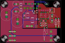
Thanks Ben. That does look nicer. But I don't know if I will be able to etch my own board with double sided trace, not to mention I dont have the skills to make such a nice PCB layout myself. And for P2p, the difficulty seems to be similar to the reference BP200 design.
With the BP200 I was infact planing to assemble the circuits in 2 separate modules, one with U1 + U2 + U5 and the second with U3 + U4 + U6. Granted I wont be able to test each sections individually.
The transformer I was planing to use was either of the two options:
Single 1kVA for both channels: Mouser #: 553-VPT48-20830; Mfr. #:VPT48-20830 =>
Parallel connection on the Primary for 115VAC; Series on the seconday. Center Tap from Red+orange connection. I'll then use a single Bridge with beefy enough forward current rating
2 330VA one per channel: Avel Lindberg Y236750 330VA 25V+25V Toroidal Transformer
Use the same arrangement as above for Center tap and bridge.
What do you think ? Reason for the 1KVA is it costs $140, if I get two 500VA they cost about $90 each. The 330VA costs $70 each ... so I'm trying to keep the cost down as much as I can
Second question about the DRV134, is there a reliable kit out there that anyone has experience with?
Also, I dont get why converting an unbalanced signal to balanced for such as short journey (from RCA jacks to Amp PCB) be necessary? From my understanding atleast the benefit of balanced is to have more gain and to have the diff amplifier eliminate interference from long signal cables
Also, I dont get why converting an unbalanced signal to balanced for such as short journey (from RCA jacks to Amp PCB) be necessary? From my understanding atleast the benefit of balanced is to have more gain and to have the diff amplifier eliminate interference from long signal cables
- Status
- This old topic is closed. If you want to reopen this topic, contact a moderator using the "Report Post" button.
- Home
- Amplifiers
- Chip Amps
- Another BPA200 post: Need some advice on finalizing design