Hi all,
A word of warning. If some of the things I did make you want to beat me with a blunt instrument, I will not hold it against you. I was (guess I still am) hasty, ignorant, inexperienced <insert your favorite profanity here>. Just trying to learn electronics and patience and humility all at the same time...
I just finished my DYI project, which was a PCB router and guess what? I wanted to make some PCBs with it . So I was looking for some fun and useful projects and stumbled upon A Complete Guide to Design and Build a Hi-Fi LM3886 Amplifier - Circuit Basics. Before I only tinkered with digital stuff, like arduinos and such, so I said, well it could be fun to try something analog.
And as much as I hate bringing up the "is this lm3886 layout ok?" topic for the umpteenth time, here it is
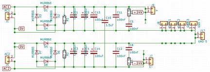
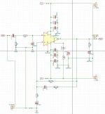
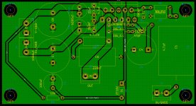
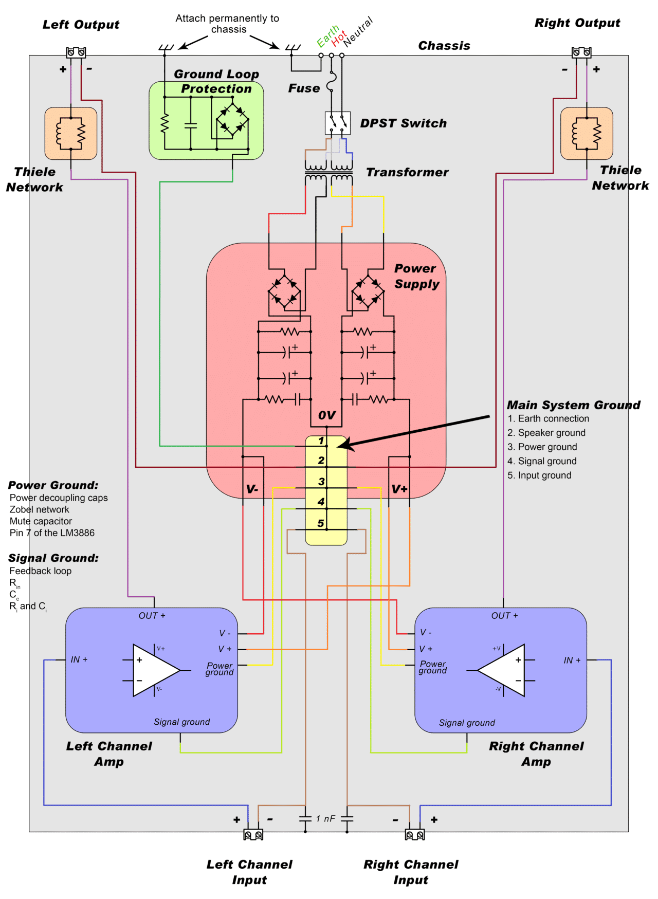
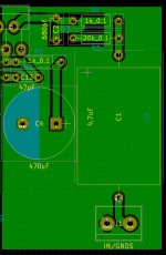
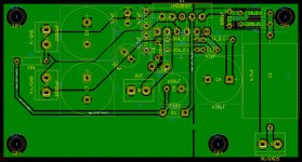
The PCB is pretty much a copy of the one from the link above, put on a single sided board. Hence the question - did I do something outright stupid while doing so? The screens of the schematic and the pcb layout of the psu and the amplifier board are attached to the post.
It's... kinda stupid of me to ask for your opinion, when the boards are already made, fitted and tested, but that's just me I guess... There are things which I'd like to ask, based on the experience during the testing of the board.
1. I used the blue screw terminals for the wiring, which I read and found out myself not to be the best thing to do - they can and will come loose and the cables can slip out pretty damn easily. It happened to me twice that the signal ground wire became disconnected while the amp was powered on with a test speaker connected. High value DC got to the output terminal. The speaker got fried. Twice. Is there something I can do to prevent DC on the output terminals in such a case, except for a speaker protection circuit?
2. Should I connect the Zobel network to the power ground or should I wire it to the PSU board individually?
3. I was picking up some digital and analog noises, because the amp was not in an enclosure. The left channel picking up mostly mobile phone signal beeping, while the right one was also picking up a radio station I was even able to identify. Those noises were rather quiet and I suppose they would mostly disappear when the amp is enclosed, right? The Thiele network is/will be connected on a separate small PCB close to the speaker terminals.
4. There was a constant high pitched noise from the speakers, rather quiet, but still something I think should not have been there. It got much quieter when I touched / enclosed the signal ground wire with my hand and also when I shifted the output cable someplace else. Didn't have much time to tinker with it, because at that moment the signal ground got loose. Bye bye speaker. I've got no more speakers left to try/fry...
5. I've read that the choice of decoupling capacitors and their values will influence sound. The how-to from the above link suggests 1000uF, 22uF, 4,7uF. What I was able to experience was rather powerful bass, maybe a little too much, but not really unpleasant. The treble I can't really tell. It was there, not harsh or anything, guess it was ok. My trouble was with the mids. Sometimes I got a feeling that the vocals are coming from behind a curtain behind the instruments. Like they were drowned by the rest of the spectrum - this was especially apparent when there was a lot going on on the stage. Listening to Dire Straits was still mostly pleasant, but some hard rock / metal tunes sounded like... noise. The vocalist tried to scream through that noise, but you had to really pay attention to spot him. And some tunes sounded significantly louder than others, probably because of the prevalent frequency range. Any suggestion you could offer to the choice of decoupling capacitors to improve the sound?
6. Last but not least I have to confess I blew up one of the lm3886 chips while trying to troubleshoot the negative rail voltage on the output. This was after I blew my last test speaker. I was trying to measure the voltages on the chip and I shorted V+ and V-, oh boy, those fireworks... Later I found some bits of solder on the back of the board I suspected blew when the chip had blown, but later I realized I was desoldering some of the caps from that board to try without them... and the bits of solder found their way to places where they should not be. Stupid me. This is a note to self - don't rush and pay attention to what you are doing and where you are doing it!
A word of warning. If some of the things I did make you want to beat me with a blunt instrument, I will not hold it against you. I was (guess I still am) hasty, ignorant, inexperienced <insert your favorite profanity here>. Just trying to learn electronics and patience and humility all at the same time...
I just finished my DYI project, which was a PCB router and guess what? I wanted to make some PCBs with it
. So I was looking for some fun and useful projects and stumbled upon A Complete Guide to Design and Build a Hi-Fi LM3886 Amplifier - Circuit Basics. Before I only tinkered with digital stuff, like arduinos and such, so I said, well it could be fun to try something analog.And as much as I hate bringing up the "is this lm3886 layout ok?" topic for the umpteenth time, here it is
The PCB is pretty much a copy of the one from the link above, put on a single sided board. Hence the question - did I do something outright stupid while doing so? The screens of the schematic and the pcb layout of the psu and the amplifier board are attached to the post.
It's... kinda stupid of me to ask for your opinion, when the boards are already made, fitted and tested, but that's just me I guess... There are things which I'd like to ask, based on the experience during the testing of the board.
1. I used the blue screw terminals for the wiring, which I read and found out myself not to be the best thing to do - they can and will come loose and the cables can slip out pretty damn easily. It happened to me twice that the signal ground wire became disconnected while the amp was powered on with a test speaker connected. High value DC got to the output terminal. The speaker got fried. Twice. Is there something I can do to prevent DC on the output terminals in such a case, except for a speaker protection circuit?
2. Should I connect the Zobel network to the power ground or should I wire it to the PSU board individually?
3. I was picking up some digital and analog noises, because the amp was not in an enclosure. The left channel picking up mostly mobile phone signal beeping, while the right one was also picking up a radio station I was even able to identify
. Those noises were rather quiet and I suppose they would mostly disappear when the amp is enclosed, right? The Thiele network is/will be connected on a separate small PCB close to the speaker terminals.4. There was a constant high pitched noise from the speakers, rather quiet, but still something I think should not have been there. It got much quieter when I touched / enclosed the signal ground wire with my hand and also when I shifted the output cable someplace else. Didn't have much time to tinker with it, because at that moment the signal ground got loose. Bye bye speaker. I've got no more speakers left to try/fry...
5. I've read that the choice of decoupling capacitors and their values will influence sound. The how-to from the above link suggests 1000uF, 22uF, 4,7uF. What I was able to experience was rather powerful bass, maybe a little too much, but not really unpleasant. The treble I can't really tell. It was there, not harsh or anything, guess it was ok. My trouble was with the mids. Sometimes I got a feeling that the vocals are coming from behind a curtain behind the instruments. Like they were drowned by the rest of the spectrum - this was especially apparent when there was a lot going on on the stage. Listening to Dire Straits was still mostly pleasant, but some hard rock / metal tunes sounded like... noise. The vocalist tried to scream through that noise, but you had to really pay attention to spot him. And some tunes sounded significantly louder than others, probably because of the prevalent frequency range. Any suggestion you could offer to the choice of decoupling capacitors to improve the sound?
6. Last but not least I have to confess I blew up one of the lm3886 chips while trying to troubleshoot the negative rail voltage on the output. This was after I blew my last test speaker. I was trying to measure the voltages on the chip and I shorted V+ and V-, oh boy, those fireworks... Later I found some bits of solder on the back of the board I suspected blew when the chip had blown, but later I realized I was desoldering some of the caps from that board to try without them... and the bits of solder found their way to places where they should not be. Stupid me. This is a note to self - don't rush and pay attention to what you are doing and where you are doing it!
Attachments
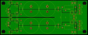
All grounds connect on the psu boardLooking at this on my mobile, so I can't see everything clearly. But where does GNDS connect to GNDPWR?
This would also cause -24V on the output.
Separated grounds according your ideas is not a good thing. They will create perfect antennas. The signal ground should sniff on the speaker ground and the speaker ground should go the power ground. Make sure you don't catch any voltage drops from the current spikes you have in the smoothing capacitors. LM3886 Done right is an example when your do the grounding correctly. LM3886 Done Right
Pavel Dudek's PA03 is also correctly designed.
Sjostrom Audio - PA03 Pavel Dudek's deLuxe Gainclone
Pavel Dudek's PA03 is also correctly designed.
Sjostrom Audio - PA03 Pavel Dudek's deLuxe Gainclone
Last edited:
@peranders I see your point with the antennas. Like I said, I didn't design this - not enough experience to do so - I followed the how-to link in the first post. Here's the link to the connection between the amps and psu from the how-to
So you suggest connecting power ground, output ground and signal ground on the amp's pcb? On Tom's PCB I see the speaker ground goes directly to the signal ground, but I can't seem to spot the connection between signal ground and power ground, because I can only see one side of the the PCB.
So you suggest connecting power ground, output ground and signal ground on the amp's pcb? On Tom's PCB I see the speaker ground goes directly to the signal ground, but I can't seem to spot the connection between signal ground and power ground, because I can only see one side of the the PCB.
Wrong.All grounds connect on the psu board
Each "ground" is a return route for a current.
Find the flow route for the current. The return route MUST follow that trace/wire all the way back to the source from whence the current started.
The pair of Flow and Return wires/traces MUST be close coupled all the way. Any increase in LOOP AREA will increase the risk of interference getting out/in from/to any current loop.
If you implement a remote ground then you force the return route to make an enormous LOOP. That is guaranteed to increase interference.
If you place the remote ground on the PSU charging circuit, that is guaranteed to make the interference even worse.
post1 pic left (1)
Remove C10 it does no good where it is.
Remove C11 it does no good where it is.
Remove C15+R5 they do no good where they are.
Reinsert a new snubber (R+C) at AC1 J1 across 1-2
Read up on transformer snubbers to find out what values of R & C your transformer might need.
Repeat for the lower side.
What value are the four electrolytics, you have done a good job of obscuring the values.
post1 pic 3
the layout of the schematic gives the impression that LOOP AREA does not matter.
look at the input circuit.
The two signal wires arrive at J1 IN/GNDS 1 & 2.
Good that they are adjacent to each other.
Now follow the Pin2 +IN through C1 and R2 back to Pin1.
See how big the LoOP AREA is !!! that must be reduced down to mm. The smaller the better.
Next look at the loop pin2 through C1, Through R1 through C2 back to pin1.
Again an enormous LOOP AREA.
Look at the input route all the way to +IN across to -IN and then back to Pin1.
The Input cables and the PCB traces must reduce those loop areas down to minuscule levels, otherwise EMI will corrupt your wanted signals.
Sort the inputs.
Now examine the output side
Look at the current route from PSU+ to amp, to speaker, to power ground and all the way back to the PSU Zero Volts. Look at the LOOP AREAS critically. Each area creates an aerial that will emit EMI.
Repeat for PSU- through to speaker and back to Zero volts.
Now repeat for the Zobel that bypasses the speaker.
Since the Zobel can only operate at very high frequencies, you need to now look at the PCB local supply rail decoupling. The high frequency changes in current that flow to the Zobel and return to the source predominantly come the decoupling. The route from the HF decoupling to the Zobel and back the the HF decoupling (for both polarities) must be capable of passing these very high frequencies. The loop area must be ultra small. The MF decoupling recharges the HF decoupling so it can tolerate small loop areas.
Sort the power wiring/traces to minimise all sources of EMI.
Last edited:
that is to protect Tomchr's Intellectual Property..........and power ground, because I can only see one side of the the PCB.
You either buy his sorted PCB and pay for his design expertise, or you learn how to do it equally well and try doing it properly yourself via one, two, or a multiplicity of prototypes.
That's why I came here. I'm beginning to see that PCB layout is not just "connect the dots"...or you learn how to do it equally well and try doing it properly yourself via one, two, or a multiplicity of prototypes.
There's some science to exactly how that plane is drawn, however. You do need to keep the sensitive signal ground quiet. You can do that in many ways. One is to use a moat (slot in the ground plane). Another is to ensure to place the parts such that the sensitive nodes are as close together as possible and in the part of the ground plane that has the lowest current density.
Tom
Tom
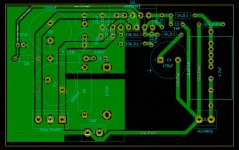
I'm back after some reading, studying other layouts and experimenting with mine. The current version is attached (C3 220pF is currently not fitted, because I don't have any handy)
I did the grounding according to tomchr's advice. I hope I understood and implemented it correctly. The best grounding scheme should be daisy chaining the grounds: Signal ground goes to Output ground goes to Power ground.
I moved the Thiele network to the pcb, as there was space available. But I've been thinking about the magnetic field the coil is creating... Currently the input
section is quite far away, but the free space there is bugging me. I'd like to move the input section a bit more to the left. Would that cause problems?
I tried keeping the loop areas small, according to AndrewT's (and others) advice. Again, I hope I succeeded at least partly.
I got rid of the ground pour on the input side and replaced it with a sort of "local star". With the ground pour there, the RF filer cap was turning the whole thing into an antenna, picking up all sorts of beeps. With the RF filter cap removed, it went quiet. With the "local star" I could keep the RF filter cap in place and the antenna effect was not so big, I could hardly hear the beeps.
The very good advice (that I found here and elsewhere) was to split the input 1k resistor in two resistors with equivalent series resistance and hook the RF filter cap in the center. This removed the picked up beeps, even with the ground pour in place.
I'm inclined to use the combination of the "local star" and split input resistor.
Attachments
- Status
- This old topic is closed. If you want to reopen this topic, contact a moderator using the "Report Post" button.
- Home
- Amplifiers
- Chip Amps
- LM3886 layout and some questions