Hi guys,
First post, but I have read a lot of comments here on the LM3886, and I've come up with a PCB that I'd like some feedback on.
Some points I'm not clear on (I've seen/read some conflicting comments on these):
1) Should PIN7 (GND) be connected to the PS ground or to the star signal ground?
2) Should the output ground return (at the terminal) be connected to the PS ground or to the star signal ground?
3) I've read somewhere that it may be better to connect the Zobel network (RSN+CSN) directly to the ground at the output terminal? Feels like this would only increase the length of the loop?
Any comments would be greatly appreciated!
Attachments
With the thick PCBs that we use for 2 layer boards, I don't think there can be any advantage in adopting one plane for one of:- Power +, or Power-, or Power Zero, or Signal Return.
Component layout rules.
That is more important than just about anything else.
They control where your traces must run. The trace/component loops control the tolerance to interference effects.
Component layout rules.
That is more important than just about anything else.
They control where your traces must run. The trace/component loops control the tolerance to interference effects.
Thanks for the input.
Would you care to give some pointers on component layout rules for the LM3886 Andrew?
I tried to keep loops as short as possible, but it seems that this is mostly dictated by the size and number of components... Inevitably it also leads to prioritizing small loops for some components over others (i.e. Rf gets priority over Rsn etc.)
Also, I'm thinking of mounting the Cc compensation capacitor on the bottom of the board since I guess the extra lead inductance would counteract the working of it. How critical is this extra inductance to avoid high frequency oscillations?
palstanturhin, I gather from your post that you recommend connecting the Zobel network to the power ground as well as the output ground. Granted the noise level is much larger at the output, but wouldn't it potentially pick up noise from the power ground?
My advice to you would be exactly the same as the advice I gave in this thread: http://www.diyaudio.com/forums/chip-amps/270206-my-take-lm3886-layout.html
If you're interested in the background, I suggest reading through my Taming the LM3886 Chip Amplifier pages. The only edit I need to make to those pages is that the "optional stability components" (Rf2, Cf, Cc in the data sheet schematics for the LM3886) actually do improve stability and should be included.
Tom
Sorry, I actually read that thread a while ago, somehow it didn't stick apparently.
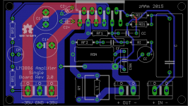
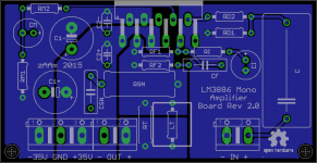
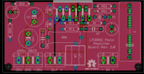
I added a signal ground plane on the top (red) and bottom (blue) layers as well as fills for all the power traces.
Cc will be soldered on the bottom of the PCB so I removed it from the board.
How does this look?
I added a signal ground plane on the top (red) and bottom (blue) layers as well as fills for all the power traces.
Cc will be soldered on the bottom of the PCB so I removed it from the board.
How does this look?
Attachments
.
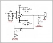
Every TI data sheet I've seen lately makes the following recommendation, slightly edited by me.
===
It is important to return the load ground, the output compensation ground, and the low level (feedback and input) grounds to the circuit board common ground point through separate paths.
Otherwise, large currents flowing along a ground conductor will generate voltages which can act as signals at the input, resulting in high frequency oscillation or excessive distortion.
===
The below illustration calls out the various grounds referenced by the data sheets.
It might be worth noting that ground planes can create more problems than they solve. The reason is that the ground plane, like all conductors, has resistance, and this resistance varies throughout the layer of copper.
This means that currents do not flow through the ground plane in an idealized smooth sheet, but take the path of least resistance from any point to any other point. The result can be unexpected inductance and/or capacitance where they will do the most harm.
The bottom line is that the factory works out its ground plane recommendations--if any--with considerable engineering expertise. Lacking such expertise using a ground plane might be something of a crap shoot, and discrete conductors to the single circuit ground point might give a better result.
On the other hand, that's a seriously good looking board you posted.
.
Attachments
For best performance, you want a low-impedance connection between the input/feedback ground and the speaker ground terminal. I pointed that out in Post #10 of the thread linked to above. You can see the difference such a low-impedance ground makes in the LM3886 P2P vs PCB (with data) thread. It's Post #30 of that thread.
Low impedance --> short, wide trace. The shortest and widest trace you can get is a plane.
Tom
Low impedance --> short, wide trace. The shortest and widest trace you can get is a plane.
Tom
Last edited:
It is important to return the load ground, the output compensation ground, and the low level (feedback and input) grounds to the circuit board common ground point through separate paths.
Which is why my recommendation is to set up a quiet section of ground plane for the signal ground (= feedback and input) and connect it to the power ground plane at the speaker connector ground connection.
Tom
...my recommendation is to set up a quiet section of ground plane for the signal ground (= feedback and input) and connect it to the power ground plane at the speaker connector ground connection.
This would be great if one could only know which parts of the ground plane are quiet, and which are not. Lacking an electron microscope I don't know how this can be done.
<< ...connect [the input and feedback grounds] to the power ground plane at the speaker connector ground connection. >>
What you mean by "the speaker connector ground connection" seems to me unclear.
If you mean connecting the return line from the speaker, the input ground, and the feedback ground all to the same point on the ground plane, that's not as recommended by some, for example as in post #8.
.
Last edited:
.
Every TI data sheet I've seen lately makes the following recommendation, slightly edited by me.
===
It is important to return the load ground, the output compensation ground, and the low level (feedback and input) grounds to the circuit board common ground point through separate paths.
Otherwise, large currents flowing along a ground conductor will generate voltages which can act as signals at the input, resulting in high frequency oscillation or excessive distortion.
===
The below illustration calls out the various grounds referenced by the data sheets.
It might be worth noting that ground planes can create more problems than they solve. The reason is that the ground plane, like all conductors, has resistance, and this resistance varies throughout the layer of copper.
This means that currents do not flow through the ground plane in an idealized smooth sheet, but take the path of least resistance from any point to any other point. The result can be unexpected inductance and/or capacitance where they will do the most harm.
The bottom line is that the factory works out its ground plane recommendations--if any--with considerable engineering expertise. Lacking such expertise using a ground plane might be something of a crap shoot, and discrete conductors to the single circuit ground point might give a better result.
On the other hand, that's a seriously good looking board you posted.
.
Thanks. I agree, if you just put a massive ground plane and connect all grounds to it, you will likely get poor results since the return paths will probably be shared somewhere between high level power and low level signals, coupling in a lot of noise/distortion. I think however that by splitting the signal and power ground planes, you should be able to get good performance?
For best performance, you want a low-impedance connection between the input/feedback ground and the speaker ground terminal. I pointed that out in Post #10 of the thread linked to above. You can see the difference such a low-impedance ground makes in the LM3886 P2P vs PCB (with data) thread. It's Post #30 of that thread.
Low impedance --> short, wide trace. The shortest and widest trace you can get is a plane.
Tom
I moved the bridge point to the output terminal, so if I understand you correctly, it should help similarly to what you tested in the PCB vs P2P thread? We should effectively have a low impedance path from the feedback directly to the output since most of the path is ground plane.
It's still impressive that such a tiny difference in impedance has such a big impact on the THD performance!
I agree, if you just put a massive ground plane and connect all grounds to it, you will likely get poor results since the return paths will probably be shared somewhere between high level power and low level signals, coupling in a lot of noise/distortion. I think however that by splitting the signal and power ground planes, you should be able to get good performance?
<< I think however that by splitting the signal and power ground planes, you should be able to get good performance? >>
You're asking me? I don't know.
However, I think at this point it's fair to ask: what's the ground plane for? What's it going to do for me that I want done?
Which is more questions I can't answer because, as you might have sensed, I'm not a big fan of ground planes. They do have their place, but it seems to me that generally they're just used as very wide wires. Why you'd want wide wires nobody seems to be able to explain.
Pop quiz: Say, "Why we want wide wires?" fast 5 times--or once.
.
Last edited:
I may have missed something, but why do you need Cc, Cf and Rf2?
Also; in theory the chips pin number 7 is the return for the mute input, so that could follow the mute signal back to its source, ie not the audio signal...
About a plane:
In a ground/power plane we assume, everything is as noisy. This noise is the same all around the board and is a nice zero reference for the chip. The chip does not know what is noise and what is not, it thinks its a nice even zero everywhere. But off course we still want to minimize that noise as much as possible even in a plane.
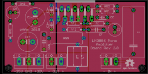
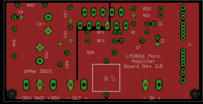
Whoops, didn't attach the new layout.
That looks pretty good. I'd extend the connection between the power ground plane and the signal ground plane all the way down, though. The current density at that spot in the power plane will be relatively low and you might as well make the connection as wide as you can get.
I suggest rotating C1+ 90 º CW and CSN 180 º to bring the grounds of the caps closer together on the plane. That'll minimize the inductance between those ground pins and control the current density in the plane.
I may have missed something, but why do you need Cc, Cf and Rf2?
Cc is needed to ensure that the LM3886 can go all the way to the supply rail without breaking into quasi-oscillation. Without Cc, you'll get oscillations near the positive peaks of the sine wave starting at about 1 V from the VCC rail. Cc gets rid of that. However, Cc causes the transient response to overshoot. Rf2 and Cf take care of the overshoot.
Also; in theory the chips pin number 7 is the return for the mute input, so that could follow the mute signal back to its source, ie not the audio signal...
The pin 7 ground is only used when the chip is muted. Unless you care tremendously about the sound quality when the amp is muted, it really doesn't matter how you route that particular ground. Personally, I connect it to the power ground because that works well in my boards.
About a plane:
I think there's a lot of misinformation regarding ground planes. It seems most people have this idea that in a wire, electrons will merrily travel single file down the wire, whereas in a ground plane, there's utter chaos and anarchy. That's pretty far from the truth. Think of a ground plane as many thin wires in parallel. The shortest route between the source and load will be the shortest thin wire. All the other wires will be progressively longer as the current paths get more convoluted. The majority of the current will take the direct route, but some of the current will take the longer routes. This means the current density in the plane will be highest in the direct path and progressively lower as you move away from the direct path.
There is nothing mythical about ground planes. They have been quite well understood since Maxwell, Faraday, and those guys came up with electromagnetic field theory some 150 years ago. It does take a bit of thinking for most people to wrap their heads around the concept, though.
Tom
Also; in theory the chips pin number 7 is the return for the mute input, so that could follow the mute signal back to its source, ie not the audio signal...
The pin 7 ground is only used when the chip is muted. Unless you care tremendously about the sound quality when the amp is muted, it really doesn't matter how you route that particular ground. Personally, I connect it to the power ground because that works well in my boards.
I've been wondering about this. The equivalent schematic shows three ground points (presumably all connected to PIN7), one of which is used for the mute transistor base, but it would seem that the other two are in operation when the amplifier is not muted (one for one side of a differential amp and one for ESD I guess). You'd think that a noisy return path for the diff amp would influence the output - it looks like it's in circuit with the input?
That looks pretty good. I'd extend the connection between the power ground plane and the signal ground plane all the way down, though. The current density at that spot in the power plane will be relatively low and you might as well make the connection as wide as you can get.
That's true, will change it accordingly.
I suggest rotating C1+ 90 º CW and CSN 180 º to bring the grounds of the caps closer together on the plane. That'll minimize the inductance between those ground pins and control the current density in the plane.
Thanks that's a good idea, we really want to contain the current paths away from the ground plane bridge.
I think there's a lot of misinformation regarding ground planes. It seems most people have this idea that in a wire, electrons will merrily travel single file down the wire, whereas in a ground plane, there's utter chaos and anarchy. That's pretty far from the truth. Think of a ground plane as many thin wires in parallel. The shortest route between the source and load will be the shortest thin wire. All the other wires will be progressively longer as the current paths get more convoluted. The majority of the current will take the direct route, but some of the current will take the longer routes. This means the current density in the plane will be highest in the direct path and progressively lower as you move away from the direct path.
There is nothing mythical about ground planes. They have been quite well understood since Maxwell, Faraday, and those guys came up with electromagnetic field theory some 150 years ago. It does take a bit of thinking for most people to wrap their heads around the concept, though.
Agreed, it's just sheet resistance basics. Lots of series/parallel squares of copper connected together.
I've been wondering about this. The equivalent schematic shows three ground points (presumably all connected to PIN7), one of which is used for the mute transistor base, but it would seem that the other two are in operation when the amplifier is not muted (one for one side of a differential amp and one for ESD I guess). You'd think that a noisy return path for the diff amp would influence the output - it looks like it's in circuit with the input?
I cover the mute circuit in some detail on my Taming the LM3886 - Grounding page.
The LM3886 has two input diff pairs. One is used during normal operation and one is use only during mute. The mute function itself is accomplished by a multiplexer that routes the bias current to either the input pair connected to the outside world (normal operation) or the mute pair (mute operation).
The Pin 7 ground is used as a reference ("input voltage") for the mute pair, reference for the multiplexer, and for a pair of clamp diodes. These diodes are not for ESD. They form a clamp that limits the differential voltage across the mute differential pair. This allows the mute pair to work faster. If the clamp wasn't there, the mute pair would likely have to recover from saturation (carrier recombination process ... sloooooowwwww) to mute or un-mute the IC.
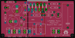
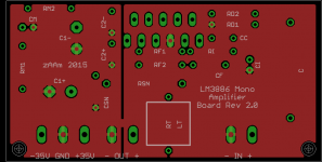
Nice layout! You get plus points in my book for including Rf2, Cf, Cc, and both Zobel and Thiele networks from the start. Nice work.
The only room for improvement I see at this point is to move the power input connector to the left side of the board. Put the mute components elsewhere. This would allow a bit cleaner supply routing and decoupling. I don't know if you're emotionally tied to having all connectors along one edge of the board, though. You don't need two mute resistors, by the way. Rmute + Cmute is all you need. The layout is nice the way it is, though. We're approaching the nit-picking stage in the review here...
")
Tom
Last edited:
- Status
- This old topic is closed. If you want to reopen this topic, contact a moderator using the "Report Post" button.
- Home
- Amplifiers
- Chip Amps
- LM3886 PCB layout questions