Yes, I see what you mean, Tomchr has no pot at all and no resistor between input and ground. It's more to demonstrate how not to mix signal returns and which leads need to be kept short.
In my case, the DC path is through the signal generator. That's legal. In your case, you don't have a DC path to ground from IN(+). The coupling cap blocks DC... You could just move the coupling cap to the input side of the pot.
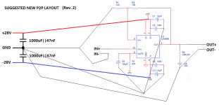
Regardless. Your layout is very similar to my suggested new layout. I see two differences:
1) I route the signal traces (input, feedback) separately to keep them away from the current returned from the load. This should improve performance as quiet ground and noisy ground are kept separate (until they hit the ground star).
2) You route the ground pin separately. That's actually not necessary. The GND pin on the LM3886 is only used for the mute circuitry (see the equivalent circuit schematic in the datasheet). Unless you care tremendously about the sound quality when the amp is muted, you can route that ground to the power ground.
~Tom
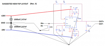
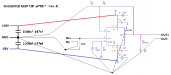
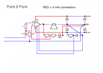
Actually... This should be a better layout. Here's why:
Signal integrity is about keeping the loop area of the current paths small. Small loop area --> low inductance of loops --> lower coupling between loops. It's also about keeping noisy signals (and remember that ground is just another signal) away from quiet signals.
The quiet signals are the input and feedback signals. The input sees a gain of 1+R2/R1, so the reason for keeping this node quiet should be pretty obvious. However, the feedback node sees a gain from the feedback "ground" to the amp output of -R2/R1, hence, injecting noise on the feedback "ground" is almost as bad as injecting the same amount of noise directly to the amp input.
The noisiest ground is the one for the load (output ground). That needs to be a separate connection to the ground star.
The decoupling ground is not super sensitive. Any RF injected on this node will probably go through the amp, but audio signals should be rejected effectively by the amp's PSRR. Running those connections separately would be trivial, so why not... Especially for P2P layout.
This thinking leaves me with attached layout. I'll try that tonight.
~Tom
Attachments
I like your explanations. Thanks. You're right. The load current does come from the bypass caps, hence, its return path should follow that of the bypass return.
I see your point about the feedback ground, but am not sure I agree. I think the feedback ground should be run separately. I'd rather avoid injecting the ground bounce back into the amp through the feedback network.
I'll try the two attached circuits and compare them against Rev. 1. I've added the DC path on the input for completeness.
~Tom
Attachments
Sometimes reading the datasheet can be helpful. Page 21:
~Tom
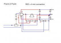
When designing a layout, it is important to return the load ground, the output compensation ground, and the low level (feedback and input) grounds to the circuit board common ground point through separate paths. Otherwise, large currents flowing along a ground conductor will generate voltages on the conductor which can effectively act as signals at the input, resulting in high frequency oscillation or excessive distortion. It is advisable to keep the output compensation components and the 0.1 μF supply decoupling capacitors as close as possible to the LM3886 to reduce the effects of PCB trace resistance and inductance. For the same reason, the ground return paths should be as short as possible.
~Tom
Now you are building something like this.
I should not post so late at night. Only the output stage is like yours the input not, out of R1 (Ri) there are two signals (loops), the feedback which goes to 0V and the input signal which goes to input return.
I should not post so late at night. Only the output stage is like yours the input not, out of R1 (Ri) there are two signals (loops), the feedback which goes to 0V and the input signal which goes to input return.
Attachments
Last edited:
Now we're cooking with gas!
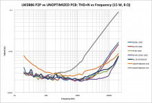
Thanks Mark. I appreciate your inputs. Based on our discussion this afternoon (your late night), I tested the attached circuits. The results were rather dramatic.
Conclusion: Layout matters greatly - also in P2P wiring (we knew that). I achieved the best performance with the IN and feedback (FB) grounds combined and returned together to the star ground. Separate IN and FB ground returns were slightly worse. Star grounding, actually, a little bit worse that the other two. NO ground return should return separately to the center point between the supply caps. Run only one wire from the ground star to this point.
Moving the Zobel network to sit directly from the IC pin to the ground star made by far the biggest improvement, closely followed by moving the IN ground to the ground star as well. That was the reason for the poor performance I was getting. My bad... The schematic for the UNOPTIMIZED P2P tested yesterday (the gray trace in the attached graph) can be found in Post #14. The Zobel network was connected across the speaker terminals (don't do that!!).
I will take the lessons learned from this and apply them to my PCB design.
~Tom
Attachments
-
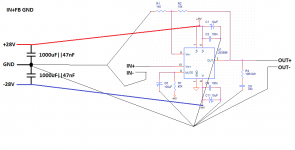 LM3886_P2P_Layout_INpFBGND.png33.6 KB · Views: 1,758
 -
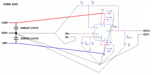 LM3886_P2P_Layout_ZobelGND.png34.9 KB · Views: 1,472
 -
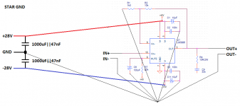 LM3886_P2P_Layout_STARGND.png32.6 KB · Views: 1,501
 -
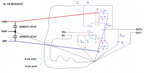 LM3886_P2P_Layout_INpFBseparateGND.png37.4 KB · Views: 1,750
 -
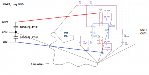 LM3886_P2P_Layout_INpFBlongGND.png36 KB · Views: 2,261
 -
 LM3886_GroundComparison.png173.9 KB · Views: 3,075
Last edited:
I was more than a bit worried that it would not work. This was all theory, I have no means to test any of this. Its a bit difficult to come to any conclusion changing both returns and PS supplies at the same time. Though it does seem to confirm that the feedback loop to 0V is more important than the input return loop.
I think there is more improvement possible by balancing the inductance (parasitics) of R1 and R2.
L(R2) should be 20 times greater than L(R1). Try to keep the gain constant from 0 to 1 MHz. Maybe closed loop gain and phase plots would help.
It does make you think, what is the point using expensive parts if you can't get your layout right. This has only cost you some time.
The impedance of a thru-hole metal film resistor is typically flat (i.e. resistive) way past 10 MHz. Yes. I've measured this. With any reasonable layout (PCB or P2P) I wouldn't worry about it.
I doubt there's much improvement to be had by changing the bypassing caps, if that's what you mean. 1000 uF || 10 uF || 100 nF is pretty close to optimum. You could add 1 nF, but I doubt it's necessary.
Exactly!
~Tom
I doubt there's much improvement to be had by changing the bypassing caps, if that's what you mean. 1000 uF || 10 uF || 100 nF is pretty close to optimum. You could add 1 nF, but I doubt it's necessary.
It does make you think, what is the point using expensive parts if you can't get your layout right. This has only cost you some time.
Exactly!
~Tom
I don't know what not to worry about, So I worry about everything.
Please can you post some photo's.
The reason I ask about caps is that there is a lot of Black art in PSU cap selection.
The biggest difference between the worst and the best P2P is the lower parasitics and maybe the separation of signals.
Please can you post some photo's.
The reason I ask about caps is that there is a lot of Black art in PSU cap selection.
The biggest difference between the worst and the best P2P is the lower parasitics and maybe the separation of signals.
Black art is only black until someone turns on the light. Lots of people want to turn the selection of passives into black art. In the end, it's about the parasitics of the selected components. Whether it's Fu-Fu Über brand or Panasonic, Nichicon, CDE brand really doesn't matter, though, from my measurements of AC coupling caps, the Fu-Fu Über brands drain your wallet faster, have worse parasitics (lower SRF, higher ESR) than the Panasonic/Nichicon/CDE brands. Of course, that's another 200-liter drum of worms that's covered in other threads and is best left unopened here... ")
I'll post pictures tomorrow.
~Tom
I'll post pictures tomorrow.
~Tom
More data.
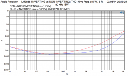
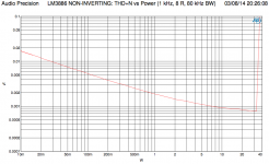
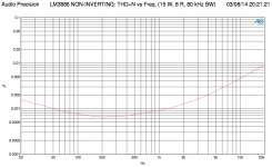
Inverting vs non-inverting configuration. The feedback network is 10k, 1k so the input impedance in the inverting configuration is too low for my THD analyzer to drive cleanly. I added an LME49710-based buffer to drive the low input impedance. The LME49710 can deliver a 3 V RMS swing into a 600 Ω load at 0.00003 % THD, so the THD in my setup is completely dominated by the LM3886. For the non-inverting configuration, I drove the LM3886 directly. Both circuits were based on my STAR GND circuit posted a few days ago.
~Tom
Attachments

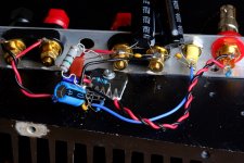
Thanks to popular demand: Pictures. Attached shows the STAR GND configuration.
Left speaker connector: Speaker output.
Right speaker connector (and yellow banana connector): Power supply.
Red RCA: Input.
The star ground point is by the blue 100 uF cap (Cmute).
In the picture, it looks like the pin of the Zobel cap (dark reddish orange) connects to VCC. That is not the case, obviously. BTW, by playing with the inductance in the Zobel (i.e. moving the resistor pin further up the cap pin), the THD is affected. That Zobel really needs to be low-inductance. That's old news to most, but it's interesting with measurements to confirm.
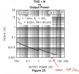
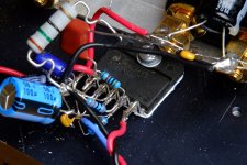
Keep in mind that this is a prototype setup. If I was to build a P2P amp, I would tighten up the connections and do a better job of soldering. But this circuit provides better performance than what's in the data sheet (probably because the AP SYS-2700 is better than the AP 2 used for the data sheet figures).
~Tom
Left speaker connector: Speaker output.
Right speaker connector (and yellow banana connector): Power supply.
Red RCA: Input.
The star ground point is by the blue 100 uF cap (Cmute).
In the picture, it looks like the pin of the Zobel cap (dark reddish orange) connects to VCC. That is not the case, obviously. BTW, by playing with the inductance in the Zobel (i.e. moving the resistor pin further up the cap pin), the THD is affected. That Zobel really needs to be low-inductance. That's old news to most, but it's interesting with measurements to confirm.
Keep in mind that this is a prototype setup. If I was to build a P2P amp, I would tighten up the connections and do a better job of soldering. But this circuit provides better performance than what's in the data sheet (probably because the AP SYS-2700 is better than the AP 2 used for the data sheet figures).
~Tom
Attachments
Last edited:
- Home
- Amplifiers
- Chip Amps
- LM3886 PCB vs Point-to-Point (with data)