Don't you read the Forum advice? You have been a Member for 4years.......Can i use Transformer 22V x 2 and 25V x 2 for this board to play 4Ohm, 8Ohm speakers?
Dual 25Vac for 8ohms capability, <dual 22Vac for 4ohms capability !
Troubleshooting Suggestions?
Happy New Year all.
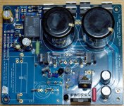
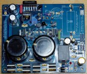
I decided to build a pair of V1.2 boards with the AD4627 opamp, JFET mods, and Evo A mods. I built them with the same components as my earlier boards, that way, I can make quick comparisons between LM318 and AD4627. Of course, I added a few additional sockets so that I can try some other components.
The build went well and all the power supply voltages are correct. With C9 still active, one board is showing less than 2 mV DC offset. However, the other board starts at about 1 VDC and slowly grows in offset. I have let it go to about 2.1 VDC before shutting it down. Interestingly, the speaker protection hasn't kicked in, so the relay and LED remain on, even above 2 VDC. This measured DC voltage is across the speaker outputs with the input shorted, nothing connected at the outlet except the meter, and C9 functioning.
I need to take and post some good pictures, but nothing appears wrong in the build. AC at the outputs is less than 2 mV on both channels, so it appears to be a DC issue.
Any suggestions on where to look?
Thanks in advance,
Jac
Happy New Year all.
I decided to build a pair of V1.2 boards with the AD4627 opamp, JFET mods, and Evo A mods. I built them with the same components as my earlier boards, that way, I can make quick comparisons between LM318 and AD4627. Of course, I added a few additional sockets so that I can try some other components.
The build went well and all the power supply voltages are correct. With C9 still active, one board is showing less than 2 mV DC offset. However, the other board starts at about 1 VDC and slowly grows in offset. I have let it go to about 2.1 VDC before shutting it down. Interestingly, the speaker protection hasn't kicked in, so the relay and LED remain on, even above 2 VDC. This measured DC voltage is across the speaker outputs with the input shorted, nothing connected at the outlet except the meter, and C9 functioning.
I need to take and post some good pictures, but nothing appears wrong in the build. AC at the outputs is less than 2 mV on both channels, so it appears to be a DC issue.
Any suggestions on where to look?
Thanks in advance,
Jac
the purpose of mod jfet is to remove C9 and connect the freed pads.Happy New Year all.
I decided to build a pair of V1.2 boards with the AD4627 opamp, JFET mods, and Evo A mods. I built them with the same components as my earlier boards, that way, I can make quick comparisons between LM318 and AD4627. Of course, I added a few additional sockets so that I can try some other components.
The build went well and all the power supply voltages are correct. With C9 still active, one board is showing less than 2 mV DC offset. However, the other board starts at about 1 VDC and slowly grows in offset. I have let it go to about 2.1 VDC before shutting it down. Interestingly, the speaker protection hasn't kicked in, so the relay and LED remain on, even above 2 VDC. This measured DC voltage is across the speaker outputs with the input shorted, nothing connected at the outlet except the meter, and C9 functioning.
I need to take and post some good pictures, but nothing appears wrong in the build. AC at the outputs is less than 2 mV on both channels, so it appears to be a DC issue.
Any suggestions on where to look?
Thanks in advance,
Jac
Hi Jac,
Happy new year to you too!
It sounds as though one channel is not stable, so you need some extra compensation in the form of a small capacitor, say 4.7pf, between pins 2 and 6 of the op-amp. A larger value of cap will do as proof of concept if you don't have such a small value.
What's the JFET mod by the way?
Dan
Hi Jac,
Happy new year to you too!
It sounds as though one channel is not stable, so you need some extra compensation in the form of a small capacitor, say 4.7pf, between pins 2 and 6 of the op-amp. A larger value of cap will do as proof of concept if you don't have such a small value.
What's the JFET mod by the way?
Dan
Hi Dan,
Thanks for your response. The JFET mod is what I called removing C34/R43. It was just an extra step from Evo A.
I will give the 4.7 pF cap a try. Is this stability issue at DC or is the DC just the result of some RF oscillation? I was incorrectly thinking an oscillation would show up as AC voltage, but I checked my meter and it's only good to 300kHz.
Thanks again.
Jac
OK, that was weird.
I soldered a 20 pF (smallest I had) across the op amp pins 2 and 6. This time, the relay didn't close, so there wasn't any DC at the out tab. There was 3.8 VAC where it was less than 2 mVAC before. Realizing that the out tab was isolated by the relay, I measured from the output end of R15 and measured -27 VDC!
Clearly this isn't the stability problem that has been found by others. Or am I wrong? I admit I don't understand how this stability issue works.
I'm starting to wonder if I hurt the op amp somehow. I'll keep looking for a difference between the boards. That -27 V takes me back to the power supply as a possibility.
I'm sure its right there in front of me, but I just can't see it. Also time for some photos.
sontero,
I know the goal is removing C9, but I didn't want to take a chance and remove it until I could make sure the circuit was OK with it in place. Hopefully, removing C9 will come later.
Jac
Most common cause for negative rail on the output is R11 going open. This should have been fixed by now.
A good guess. I put sockets in at the R11 position so that I could compare an old to new BOM. Sockets are a less reliable connection, so an open R11 could have been an issue, but I checked this and the connection is good.
To answer Spartacus' question, I only added the 20 pF and retested only the bad board.
After checking R11, I checked again. The result is a little different than I reported earlier. Measuring the output to input negative terminal (0V on the schematic) I find that the DCV is oscillating from -27 to +28 VDC on a period of about 1 seconds. When I flip over to ACV, I get various readings from 1 to 30 VAC. It looks like adding the 20 pF cap made things worse, but I still have no clue what's going on.
Jac
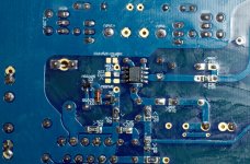
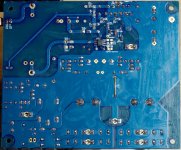
This is the board with the DC offset issue. V1.2 boards. As mentioned, I am using sockets for several resistors to be able to compare BOMs. Right now the components are from the old BOM circa 2012. I also have faston tabs for C9 and C13 so that I can use the same components on both sets of boards. I removed the caps for the photo because they block the view of the other components.
Photos below.
Photos below.
Attachments
Last edited:
Wish a happy New Year to all!
Jac, I see a very nice build..
And don't see errors.
Just some note: A load would be nice to be in place, while experimenting.
Do You have anything from 4 to 10- 15 ohm, 5 -10 - 20 W resistor..?
5W for seconds only..
May I ask had you checked the zone of LM3886 compensation, 3,3k-1nF, R37 C3x, for good contact? The same way, good continuity at the input zone, 100k; 3,3k (R12);
Finally, a smaller feedback cap would not hurt, (pin2 - pin 6, from -IN to OUT) though probably OK. (like 4,7pF)
Assume all PS are OK?
Ciao, George
Any break in any of the feedback loops will cause this. The gain will then be very high (open loop).
R11, C9, R10, R7, R3 and the connections to the IC1-3 IC2-3 are a good place to begin.
Some of the soldering topside does not look good. You want to have the solder flow on the pads and pins on both sides of the board.
R11, C9, R10, R7, R3 and the connections to the IC1-3 IC2-3 are a good place to begin.
Some of the soldering topside does not look good. You want to have the solder flow on the pads and pins on both sides of the board.
Thanks guys. Problem solved. Now a nice steady 2 mVDC offset.
I checked continuity in all the places George suggested. I touched up the soldering on several places, especially the LM3886 as Mark had suggested. I also found that I had bent the legs the little Caddock in R13 (100k) and I guess that it had developed a weak point at the bend. When I went to remove it, one of the legs came off. I'm not sure what fixed it, but if I had to guess it was either the Caddock or the soldering on the LM3886.
I appreciate the help.
Jac
PS That 2 mV was without a cap from 2 to 6 on the opamp, so the fast JFET opamps still have a pretty good record for stability.
- Home
- Amplifiers
- Chip Amps
- My_Ref Fremen Edition - Build thread and tutorial