It just occurred to me - under current swings the collector voltage on the driver transistors will be around 0.6v from the rail due to the base of the output transistor. If the VAS tries to pull the driver base higher than this, the driver obviously can't accommodate for this fact, can't turn on the output transistor any harder and becomes saturated.
The feedback diode seems to reduce this enough to stop the rail sticking, but doesn't cure the clipping spikes. An interesting problem though!
The feedback diode seems to reduce this enough to stop the rail sticking, but doesn't cure the clipping spikes. An interesting problem though!
Try a schottkey diode if you haven't. At +V clipping there should not be a current spike through R5, this means Q5 is saturating. If Q5 saturates, negative feedback becomes positive and the amplifier latches until the input swings enough the other direction to reset the LTP.
Try a schottkey diode if you haven't. At +V clipping there should not be a current spike through R5, this means Q5 is saturating. If Q5 saturates, negative feedback becomes positive and the amplifier latches until the input swings enough the other direction to reset the LTP.
Hi keantoken, I tried the diode first of all and it worked very well - I just happened to discover the other issues while probing around.
Regarding Q5 saturating - I'm not quite with you about this reversing the direction of the gain. Q11 can only pull 10s of milliamps through the base due to R5 - even at these high base currents, I don't see how the VAS voltage can fall. The current is going through the Vbe diode and Q5 is switched on as hard as it can. The output stage is already clipping at this point, so even if the gain was reversed somehow, we're already effectively in open loop conditions.
Last edited:
I could see this happening with an emitter resistor in the VAS, but the only resistance is the inherent emitter resistance of the transistor, which is probably way too small to have this effect, and rise enough voltage to 'un-clip' the output stage to cause positive feedback
It does not matter how much gain there is as long as it is reversed. If it reverses, it's positive feedback period. It will cause the circuit to latch. Q11 may be limited by R5 but until that point readily saturates Q5.
What do the spikes look like? Those TIPs are super-slow and clunky, they are probably complaining very loudly when saturating. You might try probing R8 and R15.
What do the spikes look like? Those TIPs are super-slow and clunky, they are probably complaining very loudly when saturating. You might try probing R8 and R15.
That makes sense. Remember the VAS gain corner is probably in the 100s of Hz. This means the miller cap is effectively huge compared to the impedance at the VAS input. Therefore if this cap gets charged due to a glitch, it will take a long time before it can discharge and reset the circuit. Getting rid of the current mirror drastically lowers VAS input impedance.
This is one of the reasons I don't like large miller caps. One thing you can do if you think distortion is already good enough, is to degenerate the input stage in order to make the miller cap smaller. Furthermore, I believe you can also lower the miller cap if you trade the outputs for an MJE1503x pair which will be faster and cause less second-order loading of the frontend.
This is one of the reasons I don't like large miller caps. One thing you can do if you think distortion is already good enough, is to degenerate the input stage in order to make the miller cap smaller. Furthermore, I believe you can also lower the miller cap if you trade the outputs for an MJE1503x pair which will be faster and cause less second-order loading of the frontend.
Last edited:
The diode from VAS output to buffer input works great, but I'm going crazy trying to figure out WHY it works. Without it, the current mirror goes unbalanced during the sticking period, but with it, it feeds some current into the input side LTP. This brings the current mirror back into balance, somehow.
Interesting. Sometimes current mirrors are misapplied so that Q9 will saturate, but that is for the negative excursion and doesn't seem to apply here. Also, current mirrors in this position need transistors with good quasi-sat curves. BC5xx and BC3x7 are good. 2N5550 and 5400 are often used here but really shouldn't. The datasheets don't show Vcesat behavior for the 2N390x.
What is the Vbe mismatch between Q10 and Q9? It will suffice to probe between the emitters with a DMM while the amp is running with no input. Despite the 56R degen the CM will unbalance at very low currents, even if it is not saturating, as a result of any significant Vbe mismatch. But current should only get this low during clipping. How much does the current mirror unbalance?
What is the Vbe mismatch between Q10 and Q9? It will suffice to probe between the emitters with a DMM while the amp is running with no input. Despite the 56R degen the CM will unbalance at very low currents, even if it is not saturating, as a result of any significant Vbe mismatch. But current should only get this low during clipping. How much does the current mirror unbalance?
This has all been in simulation BTW.
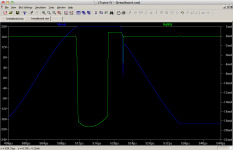
Weirdly enough, it doesn't seem to be a drive issue. During the sticking period, the VAS driver abruptly stops feeding the base, until the voltage drops back within the rails, yet the VAS stays on for a period of about 4 microseconds. If I change the VAS transistor to a BC557, the rail sticking stops, even without a diode.
Weirdly enough, it doesn't seem to be a drive issue. During the sticking period, the VAS driver abruptly stops feeding the base, until the voltage drops back within the rails, yet the VAS stays on for a period of about 4 microseconds. If I change the VAS transistor to a BC557, the rail sticking stops, even without a diode.
Last edited:
That is strange. Use these models for your simulations, only use other models if you're desperate. Ask me if you want more models. See if these models do the same thing. They were created by Cordell and should work properly.
CordellAudio.com - SPICE Models
CordellAudio.com - SPICE Models
That is strange. Use these models for your simulations, only use other models if you're desperate. Ask me if you want more models. See if these models do the same thing. They were created by Cordell and should work properly.
CordellAudio.com - SPICE Models
Oh thank god for this - I just had a look in standard.bjt and the included LTSpice 2N3904 model seems to be missing most of its parameters. I will try these soon. I'm not determined to use a 2N3904 in this position, it just irks me that it seems to be transistor dependant.
different models will give different results in simulation.
I can see the shadow lengths cast by two flagpoles are different.
But I think the models I used were the same. Why should the shadows be different?
I'd better climb up the flagpoles and drop a weight off yet again to check the time of flight (height) of the two poles. The models are probably different !
Same with semiconductors. Can't measure them directly, we measure parameters and hope the parameters will allow us to simulate as accurately as is needed to answer the questions we ask the simulator.
Last edited:
")
Some designers know the behavior of all the components well enough to determine the circuit's basic behavior and specifications pretty well. This does not really take a simulator in most cases, but if a person can do this well without a simulator, they should at least be able to do as well with one. The problem is that most of our so-called "models" were generated by a computer and something went terribly wrong. To this day these errors never have been corrected or payed mind to.
I think there is even an element of fraud. I found some Fairchild models for a complementary power transistor pair. The two models were obviously the same, except some parameters had numbers transposed and stuff to give the illusion they were both generated individually. There are also many models that have different part numbers, but the same parameters and this is totally bogus.
I don't know, maybe MODPEX is a huge filthy stinking scam? Did someone get rich off of commissions from the semiconductor manufacturers?
It might be just that the models are just a token effort, and in real life things get prototyped with components that ought to work - and if they are found not to, they get swapped out. Something could work amazingly in simulation and just not perform in real life due to real circuit layouts, real tolerance spreads, etc.
Regarding fast output transistors, I don't quite get the need for super-quick ones - amps with the good old 3055 sound pretty good afterall. I know Ft drops with low Iq, but real amps still seem to work? I might be missing something.
Regarding fast output transistors, I don't quite get the need for super-quick ones - amps with the good old 3055 sound pretty good afterall. I know Ft drops with low Iq, but real amps still seem to work? I might be missing something.
In a real AB amp, combined Q never goes below 80mA, so effective Ft in the crossover region is still relatively high. Furthermore, with a higher bias point the outputs are given more time to turn on and off. If Ft is too small in the crossover region your amp's BW and stability characteristics will dramatically change during excursions, and you may get anomalous stability problems.
However, if Ft is relatively high for both crossover and excursions, you can make the amp faster because compensation is not trying to hit a moving target. Faster amp means less compensation means less distortion. I do it because I want to have the same AC behavior at all operating points.
Faster outputs are easier to drive, so they don't saturate preceding stages on RFI, causing operating point jumps and intermodulation. They are quicker to recover from clipping and saturation because they don't store so much energy in their junctions.
- Status
- This old topic is closed. If you want to reopen this topic, contact a moderator using the "Report Post" button.
- Home
- Amplifiers
- Chip Amps
- Contest: Linear Power Amp in a mint tin (class Aa, class AB, or class B)