Hi everyone,
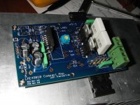
This is my new 49810/49811 + ThermalTrak Amp intended for low output power (Class-AB/B, <= 60 W). Output stage is driver + emitter follower. I have not put the heatsink for LME and driver (too noisy to do metal work in the midnight).
This is my new 49810/49811 + ThermalTrak Amp intended for low output power (Class-AB/B, <= 60 W). Output stage is driver + emitter follower. I have not put the heatsink for LME and driver (too noisy to do metal work in the midnight).
Attachments
Last edited:
Panson,
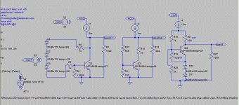
I got both my Leach bais configuration and Cordell bais configuration for thermal trak working. The Cordell is tweaked a bit from his diagram - I decided to simulate both schemes to see how they react to temperature.
The values shown were adjusted to 2.93v at 27deg c. Then I changed the simulation temperature to 68deg c and ran it again. You can see that the Cordell version stays closer to the baseline Vbe which assumes that the Vbe transistor has a perfect thermal connection to the output transistors.
Ken
Attachments
Panson,
I got both my Leach bais configuration and Cordell bais configuration for thermal trak working. The Cordell is tweaked a bit from his diagram - I decided to simulate both schemes to see how they react to temperature.
The values shown were adjusted to 2.93v at 27deg c. Then I changed the simulation temperature to 68deg c and ran it again. You can see that the Cordell version stays closer to the baseline Vbe which assumes that the Vbe transistor has a perfect thermal connection to the output transistors.
Ken
Hi Ken,
Nice work! Have you tested the bias control in real circuit?
Hi Ken,
Nice work! Have you tested the bias control in real circuit?
Panson,
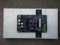
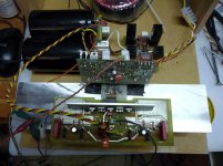
Yes, using your modular approach, I now have three boards, the LME49811, with DC Servo, a board for the bias resistors, and the output board which contains the VBE transistor, predrivers, drivers and Thermal trak output devices. I put jumpers at the T Trak so that I can use either two, three or four of them in series. I had to make some mods to the driver board to go from the Leach bias scheme to the Cordell scheme. The photo shows the Cordell scheme. Note that I had to put pairs or resistors in series to get the correct resistance. Seems you never have the right stuff on hand regardless of biweekly DigiKey and Mouser orders...
My shop computer with the highend sound card died, so, no THD tests for a few weeks. But, played it with both bais schemes and it sounds great, also, sine and square waves look smooth and clean on the scope.
Ken
Attachments
Playing Santana CD
One set of compact amp is setting in the lab for daily use. It is now playing Santana YouTube - PansonAudio's Channel
The operating voltage is +/- 35 V. The speaker is NHT SuperTwo (http://www.stereophile.com/floorloudspeakers/1099nht/).
One set of compact amp is setting in the lab for daily use. It is now playing Santana YouTube - PansonAudio's Channel
The operating voltage is +/- 35 V. The speaker is NHT SuperTwo (http://www.stereophile.com/floorloudspeakers/1099nht/).
Last edited:
One set of compact amp is setting in the lab for daily use. It is now playing Santana YouTube - PansonAudio's Channel
The operating voltage is +/- 35 V. The speaker is NHT SuperTwo (Stereophile: NHT SuperTwo loudspeaker).
Panson,
Nice little video, made me smile. I also looked at the cross over distortion video. I presume that you are showing the bais trimming out the distortion. Is this measured just with the scope? Or how do you set up for this measurement?
Thanks
Ken
Panson,
Nice little video, made me smile. I also looked at the cross over distortion video. I presume that you are showing the bais trimming out the distortion. Is this measured just with the scope? Or how do you set up for this measurement?
Thanks
Ken
Ken,
Yes, it is. The cross-over waveform is the THD residual from the AP output (after the notch filter).
Panson
Ken,
Yes, it is. The cross-over waveform is the THD residual from the AP output (after the notch filter).
Panson
Well, I guess I won't be doing that anytime soon...
Ken,
Yes, it is. The cross-over waveform is the THD residual from the AP output (after the notch filter).
Panson
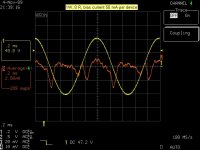
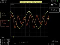
What is the bias current to get the optimum result ?
What is the bias current to get the optimum result ?
Peter,
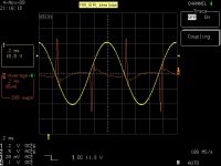
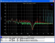
I have some more data which should be able to answer your question. The output waveform (1W/8Ohm) and THD residual are monitored for various bias levels. FFT of the residuals are also shown in the figure.
You can see very large spikes of cross-over distortion for zero bias. When the bias current is 50 mA per device, the cross-over distortion is reduced substantially (notice the vertical scale). At 100 mA bias level, we see no more cross-over distortion. The distortion is mainly contributed by 3rd harmonic.
I use 0.22 Ohm emitter resistors (Re) for the output devices. The voltage drop is 22 mV. Optimum Vq (2 Re drop) for EF is 42 mV, as given in Self's book. Here is 44 mV, more less the same. This is the optimum value.
Panson
Attachments
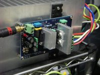
Looks like have drivers... mje15030/31?
Quick question, how does one know or determine right size resistor that is often strung betweeen the emitter's of the top and bottom driver, before it feeds the gate resistors?
What happens if not have in place?... sorry for off topic, but cannot find much info about creating driver. Wish to run 3-4 parallel mosfets.
In an1645 doc they show a 100ohm but tied to output rather than to other driver emitter.
Looks like have drivers... mje15030/31?
Quick question, how does one know or determine right size resistor that is often strung betweeen the emitter's of the top and bottom driver, before it feeds the gate resistors?
What happens if not have in place?... sorry for off topic, but cannot find much info about creating driver. Wish to run 3-4 parallel mosfets.
In an1645 doc they show a 100ohm but tied to output rather than to other driver emitter.
Yes, the drivers are 15030/31.
That resistor value can be determined by how much standing is going to pass the driver transistors. I have 1.226 V across 180 Ohm. Hence, the driver bias current is 6.8 mA. The voltage drop across this resistor together with the emitter resistors of output devices sets the output bias current. You simply can't without it.
You can find some information from this link regarding Leach Amp The Leach Amp - Output Stage. Look for R34, 35, 36.
The driver design in AN1645 is something like Darlington.
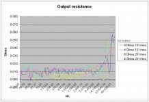
Output resistance
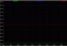
I measured the output resistance. Output circuit output voltage was set to 10 Vrms, 1 kHz. The AP recorded the output level without loading from 10 Hz to 50 kHz. The output level was then measured again for 8 Ohms and 4 Ohms load. The amplifier output resistance is estimated by using the measured data. The measured was repeated for output level set to 20 V rms, unloaded.
It can be seen that the output resistance in audio band is below 20 mOhms. Damping factor, ignoring cable effect, is > 400 for 8 Ohms.
Attachments
Last edited:
Peter,
I have some more data which should be able to answer your question. The output waveform (1W/8Ohm) and THD residual are monitored for various bias levels. FFT of the residuals are also shown in the figure.
You can see very large spikes of cross-over distortion for zero bias. When the bias current is 50 mA per device, the cross-over distortion is reduced substantially (notice the vertical scale). At 100 mA bias level, we see no more cross-over distortion. The distortion is mainly contributed by 3rd harmonic.
I use 0.22 Ohm emitter resistors (Re) for the output devices. The voltage drop is 22 mV. Optimum Vq (2 Re drop) for EF is 42 mV, as given in Self's book. Here is 44 mV, more less the same. This is the optimum value.
Panson
Oops, let me try again...
Panson, I could really use your help. My amp is running, sounds great, makes nice sine and square waves at 1k, 10k and 20k hz. So, I can't for the life of me measure the voltage drop across Re. Here's how I'm set up for the measurement: power on, input shorted, DMM probes set at emmitter of pnp and npn output transisitors, reading is 0v. If I put the probe at the emmitter of either transistor and ground, I get .006v, at the base of either transistor I get .475v.
Any thoughts?
Thanks,
Ken
Ken,
Are you using Leah triple output stage and Vbe multiplier? Based on your values, I believe the output transistors do not turn on. Can you measure base-to-emitter voltage? the base to emitter should be above 0.5 V when the device is active. What is the bias voltage generated by the Vbe multiplier? Do you have a potentiometer for bias level trimming? When you measured, was the output connected to a speaker, float or a dummy load (8Ohms)?
Panson
the voltage acros one Vbe should be +ve and the other should be -ve.DMM probes set at emmitter of pnp and npn output transisitors, reading is 0v. If I put the probe at the emmitter of either transistor and ground, I get .006v, at the base of either transistor I get .475v.
You say both are 0.475Vdc is either -ve or both +ve.
Measure from emitter to emitter of the output pair.
Measure from base to base of the output pair.
Measure from base to base of the driver pair.
Oops, let me try again...
Panson, I could really use your help. My amp is running, sounds great, makes nice sine and square waves at 1k, 10k and 20k hz. So, I can't for the life of me measure the voltage drop across Re. Here's how I'm set up for the measurement: power on, input shorted, DMM probes set at emmitter of pnp and npn output transisitors, reading is 0v. If I put the probe at the emmitter of either transistor and ground, I get .006v, at the base of either transistor I get .475v.
Any thoughts?
Thanks,
Ken
Assuming you measure the voltage across the Re without signal, then your measurement shows underbiasing. Vbe < 0.6V so no bias current so no drop across Re. Increase the bias until you see Vre rising, until you have the desired bias current.
jd
- Home
- Amplifiers
- Chip Amps
- Compact Sized LME49810/11 +ThermalTrak Amp