Yep, that is correct. Was planing to do that, can't believe I missed that one.To have only one connection between power and signal ground, I wouldn't connect the ground of J1 to the top groundplane.
BTW it's easier to understand a PCB if you don't mirror the bottom.
Thank.you on that!
Some time ago I also started with a LM3886 layout.
Never finished, but maybe I will continue after reading this tread, some good information here. Still need to beef up the power traces and add groundplane(s).
I am new to this but I recommend you read the following material several times as it helped me a lot:
TI Datasheet
tomchr's guide on LM3886
Wikipedia on operational amplifiers
Various lm3886 diyaudio threads
The layout you have is pretty much point to point wiring.
I would start with the new layout.
Keep attention to grounding layouts(reduced loops, separated signal and GND layout that connect the the speaker out) and supply decoupling as they are vital to LM3886 performance as those are vital if you want to achieve LM3886 datasheet performance.
Happy diy-ing!
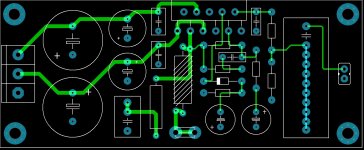
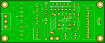
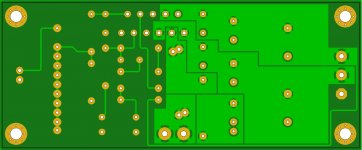
I added the groundplanes and beefed uo the high current tracks.
Not sure where to connect the power groundplane to the signal groundplane though.
Attachments
")
The only component that crosses over the cut between the planes is the chipamp.
Or is there a component that I can't see crossing over?
That points to the trace under the chipamp as the place to make the connection.
Yes, the LM3886 is the only part crossing the split between the planes. Thanks for the insight.
LM3886 Preamp
I made PCB for LM3886 few posts before.
This is the schematic

I would also add volume control with current buffering after the potenciometer. Buffer would be something like OPA2134 and and lm317 to drop the voltage from the +-30V main amp psu.
So just a basic and simple board that goes - input/potenciometer/opmap that wires to the amp board.
Are there any more modern op amps that would server this purpose and are there better solutions to bringing down the +-30V for the buffer supply?
I made PCB for LM3886 few posts before.
This is the schematic
I would also add volume control with current buffering after the potenciometer. Buffer would be something like OPA2134 and and lm317 to drop the voltage from the +-30V main amp psu.
So just a basic and simple board that goes - input/potenciometer/opmap that wires to the amp board.
Are there any more modern op amps that would server this purpose and are there better solutions to bringing down the +-30V for the buffer supply?
Bozoc,
Most of the three way trace intersections are highlighted with a big dot.
One of the NFB and both inductor intersections are missing the dot.
Does the software know these are connected?
Starting on the far left, the first resistor is connected between signal Hot/Flow and Cold/Return.
I think the next resistor (R1?) should also be connected likewise.
The capacitor at the bottom (C3) on the NFB lower leg allows the differential input of the opamp to measure the input voltage across the two signal leads. But you have it connected to the Power Ground (GNDPWR). I think the lower leg of the NFB needs to be moved up beside R2? (the third resistor from the left) and connect to R1? and to Signal Cold/Return.
The LOOP AREAS of all these INPUT components and traces must be minimised.
Back to differential signalling. The opamp/chipamp/poweramplifier are all differential input devices. These measure the voltage of the Signal at the Input, process that signal and send a scaled version to the Output.
The NFB takes a part of the output, scales it down and mixes that with the Input signal to set the stage gain and minimise noise and distortion. The NFB connects the OUTPUT to the INPUT.
Add an RF attenuation filter to the Input. Think about adding RF attenuation filters to all the cables entering the enclosure.
Associated with this interference attenuation, consider adding a Zobel across the output/speaker terminals at the enclosure exit. This can be 5r+100nF
With the added 5r in that final Zobel you can reduce the resistor value across the Output Inductor. Change it to 5r to make the TOTAL resistance equal to your preferred value.
These two resistances (in series) are in parallel to the output Zobel R7+C17
The amplifier has to drive both at HF. Thus you can increase R7 very slightly to bring the combination up to the value that National recommend.
And you get the benefit of attenuating interference picked up on the speaker cables before it is injected into -IN node.
Last edited:
Thanks Andrew.
Was also wondering about that, but software does not highlight the dot if you connect two or more wires to the component pad of the component, but connects everything.
Still learning how to use the KiCad.
If I use seperate PWR ground and SIGNAL ground KiCad does not let me connect them when working on the layout, and if they are connected in the schematic everything gets messed up.
I just use PWR GND this way and avoid problems. I do however pay attention to the layout itself.
Pretty sure I read that connecting C3 to the power ground yields better THD, maybe I am wrong but I was the thread where LM3886 gets tested with point to point layout, I will try to find that.
Here is the schematic that is slightly touched up and the last version of the gerbers I made:


Most of the three way trace intersections are highlighted with a big dot.
One of the NFB and both inductor intersections are missing the dot.
Does the software know these are connected?
Was also wondering about that, but software does not highlight the dot if you connect two or more wires to the component pad of the component, but connects everything.
Still learning how to use the KiCad.
The capacitor at the bottom (C3) on the NFB lower leg allows the differential input of the opamp to measure the input voltage across the two signal leads. But you have it connected to the Power Ground (GNDPWR).
If I use seperate PWR ground and SIGNAL ground KiCad does not let me connect them when working on the layout, and if they are connected in the schematic everything gets messed up.
I just use PWR GND this way and avoid problems. I do however pay attention to the layout itself.
Pretty sure I read that connecting C3 to the power ground yields better THD, maybe I am wrong but I was the thread where LM3886 gets tested with point to point layout, I will try to find that.
Here is the schematic that is slightly touched up and the last version of the gerbers I made:
- Status
- This old topic is closed. If you want to reopen this topic, contact a moderator using the "Report Post" button.
- Home
- Amplifiers
- Chip Amps
- LM3886 Layout ok?