Hi all, I'm just about to get started with my first DIY project. I've spent a lot of time reading but I thought I'd just get some feedback on my pcb-layout etc before i get to work.
PSU:
-----
Tx: 120 VA 2x18~
Filtered by anything from 1000 to 6600uf per rail (ill probably start with 3300 per rail As that is what i have available now)
Amp
-----
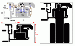
I'm using the schematics from Elliots site (Project no 72) but want to do my own boards. The layout is made in eagle and I've attached a picture.
Do you think the overall layout and specifically the grounding scheme is good, and what about the trace thickness? (signal traces 40 mil, power lines 100mil)
Components:
-----------------
What do people prefer for C1 ? bipolar electrolytic or some other type of capacitor?
Also, any specific concerns about the components in the zobel? film or ceramic?
that's it for now i guess..
thanks,
PSU:
-----
Tx: 120 VA 2x18~
Filtered by anything from 1000 to 6600uf per rail (ill probably start with 3300 per rail As that is what i have available now)
Amp
-----
I'm using the schematics from Elliots site (Project no 72) but want to do my own boards. The layout is made in eagle and I've attached a picture.
An externally hosted image should be here but it was not working when we last tested it.
Do you think the overall layout and specifically the grounding scheme is good, and what about the trace thickness? (signal traces 40 mil, power lines 100mil)
Components:
-----------------
What do people prefer for C1 ? bipolar electrolytic or some other type of capacitor?
Also, any specific concerns about the components in the zobel? film or ceramic?
that's it for now i guess..
thanks,

paswa, thanks for the comments. first, just to clarify, the schematics is from Elliots site, the PCB is not, it is my own layout.
yes i think signal ground and power ground will be connected. I'm still not sure where they will connect though. maybe with a jumper on board or maybe at the central star ground point. I may have to experiment a bit with this...
I've seen lots of people putting a resistor between the actual ground point and the grounding pad on the PCB, not reallty sure why so if anyone can explain this i'd be happy. Is it in order to limit current-sharing between for example signalpath and the powersupply?
i'm ordering parts now and hope to etch my boards soon.
leolabs, i planning to use a shared heatsink for the pair of IC's. the heatsink is roughly 100x75x20mm and specified at 1.5C/W at 50W which should be enough right?
signal ground
hi had some time off recently and have built a couple of chip amps namely TDA 2030, 2040 and 2050, incedentaly the 2050 has same pinouts as the LM1875. you want to have the ground lifted slightly for the signal as this helps to prevent a high current(from your power ground) being carried into your inputs, if you ground your inputs onto the supply ground bad sound, and possibly high DC offset at the speaker may result, with the associated unpleasant side effects, trust me separate tracks and a jumper work really well made four amps so far and background noise almost nonexistant by the way if your power supply is robust enough 3300uf is ok but 6000 always better.")
hi had some time off recently and have built a couple of chip amps namely TDA 2030, 2040 and 2050, incedentaly the 2050 has same pinouts as the LM1875. you want to have the ground lifted slightly for the signal as this helps to prevent a high current(from your power ground) being carried into your inputs, if you ground your inputs onto the supply ground bad sound, and possibly high DC offset at the speaker may result, with the associated unpleasant side effects, trust me separate tracks and a jumper work really well made four amps so far and background noise almost nonexistant by the way if your power supply is robust enough 3300uf is ok but 6000 always better.
hpl said:Hi all, I'm just about to get started with my first DIY project. I've spent a lot of time reading but I thought I'd just get some feedback on my pcb-layout etc before i get to work.
PSU:
-----
Tx: 120 VA 2x18~
Filtered by anything from 1000 to 6600uf per rail (ill probably start with 3300 per rail As that is what i have available now)
Amp
-----
I'm using the schematics from Elliots site (Project no 72) but want to do my own boards. The layout is made in eagle and I've attached a picture.
An externally hosted image should be here but it was not working when we last tested it.
Do you think the overall layout and specifically the grounding scheme is good, and what about the trace thickness? (signal traces 40 mil, power lines 100mil)
Components:
-----------------
What do people prefer for C1 ? bipolar electrolytic or some other type of capacitor?
Also, any specific concerns about the components in the zobel? film or ceramic?
that's it for now i guess..
thanks,
Hi hpl,
You've made a good start on the PCB. But there are some things that I think you might want to change, if you do another version. (Note that I have not checked the actual connection topology, versus a schematic. I only looked at the PCB layout issues.)
I would want to get the large electrolytic caps as close as possible to the chip's power pins. You could move the large input cap and all of the other input stuff to the left and/or upward, and put the big electros right up by the smaller bypass caps. You will probably want to leave enough room to be able to use up to at least 1000uF for the electrolytics, there, and maybe even 2200 uF. [The Nichicon low-ESR UHE-series, for example, has a 50V 1000uF model with a 12.5mm diameter (but 40mm height), with 5 mm lead spacing, and also 1000uF (w/20mm height) and 2200 uF (w/35.5mm height) models that have 18mm diameter and 7.5 mm lead spacing. (Their mouser.com part numbers all start with 647-UHE1H, with the remainder being 102MHD or 102MHD3 or 222MHD6.)]
You should probably also give the Zobel's R6 its own separate ground return, back to the star ground point (and probably also connect the speaker's negative terminal to that pad, on this board, so the zobel is directly across the speaker output terminals), which could also help make it easier to move the large caps closer to the chip.
After you build it, you might want to also try soldering a 0.22uF or so film cap directly between the LM1875's power pins, or on the bottom of the board. You could enlarge the traces around the power pins pads, in case you'd rather drill holes for that, instead of soldering directly to the power pins.
Usually, it's a good idea to not have any traces joining with acute angles (i.e. less than 90 degrees). PCB manufacturers call those "acid traps", and they can cause etching problems. So, after you move the large caps closer to the chip, you should probably revise the way the bypass caps' ground traces connect to each other.
You will NOT want to join the signal and power grounds, except at the star point.
I would also try to keep the V+ and V- traces as close together as possible, along with their bypasses' ground return trace, to minimize the loop areas, which should help to minimize field-induced problems. The three power and ground wires should be tightly twisted together, on their way to this board, too. The same idea should also be applied to your signal input and signal ground traces and wires.
I see that you have what looks like a lowpass RF filter for the signal input. Very good. You might want to consider moving it so that its capacitor is directly at the LM1875's positive input pin.
If you want to make the power, ground, and output traces even fatter, that won't hurt anything, either. You could also fatten the signal traces by 50% or more.
You might also want to think about using some type of wire-to-board connectors, and leave room (and matching hole sizes and spacings) for them. Soldering the wires directly to the board often turns out to be very inconvenient, later. Some small terminal blocks might be easy. I'd use two-position ones for the input signal/ground and speaker output/gnd, and a three-position one for V+/Gnd/V-. Examples: mouser.com # 651-1935161 (2 pos) and 651-1935174 (3 pos), which have 5 mm lead-spacing
The speaker ground wire (connecting to Zobel's gnd) and the separate ground wire from there to the star point would have to share a spot in the terminal block, which shouldn't be a problem. But it might be, with some other connector type. You could also just use a three-position connector, there, with the two gnd positions connected by a fat pcb trace.
Leolabs said:Wonder why not put the zobel network directly at the speaker terminal???Save some space on the PCB.
I have heard of that being done. But I think that the Zobel network should probably be right at the chip's output, in this case.
Here is a quote from the LM1875 datasheet, where, by "output compensation components", they are referring to the Zobel network:
"It is advisable to keep the output compensation components and the 0.1 µF supply decoupling capacitors as close as possible to the LM1875 to reduce the effects of PCB trace resistance and inductance. For the same reason, the ground return paths for these components should be as short as possible."
Tom,
thanks for the excellent input. I'll spend some time reading your comments and think about how to implement them.
But, regarding the filtering caps, i think it is my fault for being unclear, the electrolytics seen on board are not the main filtering caps, these are mounted off the PCB together with the rectifier bridge and a pair of fuses. I should have made this clear from the beginning. The caps on the PCB is a pair of 100uF electrolytics.
I'll read this through a couple of more times, i might have some extra questions then..
hpl said:Tom,
thanks for the excellent input. I'll spend some time reading your comments and think about how to implement them.
But, regarding the filtering caps, i think it is my fault for being unclear, the electrolytics seen on board are not the main filtering caps, these are mounted off the PCB together with the rectifier bridge and a pair of fuses. I should have made this clear from the beginning. The caps on the PCB is a pair of 100uF electrolytics.
I'll read this through a couple of more times, i might have some extra questions then..
Hi hpl,
Thanks for the response. You're welcome.
I realized that those caps were not the power supply filter caps. But I think that you will still probably want to leave space for a minimum of 1000 uF, for them, which is the value recommended on page 8 the LM1875 datasheet, available at national.com. (Aside: Note that in the figures on page 8 of the LM1875 datasheet, the component layers should be shifted up and to the left, to align with the pcb trace layouts shown.)
I have heard that this chip family is sensitive to inductance at their power supply pins. That is one reason to try to get the large electrolytics closer to the power supply pins. Smaller-diameter electrolytics will also have lower parasitic inductance, which, in most modern electrolytic caps, is mainly only due to the distance between the leads.
If possible, I would leave room for accommodating even larger electrolytic sizes. You can just make an extra pad for each one, for the larger lead-spacing option. The thinner 12.5mm-diameter 1000uF caps that I mentioned shouldn't be too difficult to leave room for. But the 18mm sizes might tax your layout just a bit. I think it can be done, though, especially if you scrunch the power and power ground traces together, as far to the right side as possible, and rearrange your signal components and traces, as far to the left as possible. Try to remember to also keep your signal traces and components as far away from the power traces as you can, for as long as you can.
What type and value of input capacitor have you depicted? Finding a differently-sized one that is at least as good should help with the layout. If you mention the type and value, people here should be able to help with the selection. Note that that capacitor should probably be non-polar or bipolar. A film type would probably be best, there.
By the way: If you haven't already done so, I recommend ordering the free paper catalogs from mouser.com and alliedelec.com . They are fantastic references to have on hand; extremely useful.
MJS said:This is my PCB of Elliot´s eschematics
On the right part of the image i added the power supply rails
Regards
Hi MJS,
I like it! Your grounding scheme looks very good.
I am not sure where your speaker ground return is connected. I guess it should be near the Zobel's ground. And I can see a few probably-minor possible changes, to better-define the star ground point and to better-segregate the ground-return currents, and to otherwise tighten things up a bit. But if you don't have any hum or distortion, they would probably just amount to nitpicking. So I won't even mention them.
Good job.
Yes, near de ZObel´s ground, but i havent electronics knowledge, if you have a good idea please tell me
No hum, no noise, it sounds very good, and very good bass
I´m trying to make a 8 channel amp for multiamplification, my idea is Bass with LM3886, middle with Tube Gainclone and treble with LM1875, but i will decide when i finish all prototypes
A friend make me two amps and active filters for the stereo sub´s
Regards
MJS said:Yes, near de ZObel´s ground, but i havent electronics knowledge, if you have a good idea please tell me
No hum, no noise, it sounds very good, and very good bass
I´m trying to make a 8 channel amp for multiamplification, my idea is Bass with LM3886, middle with Tube Gainclone and treble with LM1875, but i will decide when i finish all prototypes
A friend make me two amps and active filters for the stereo sub´s
Regards
Hi MJS,
Well, this is hpl's thread, about his pcb layout. I think we would be hijacking hpl's thread, if we started discussing details of possible changes to a completely different pcb layout.
If you want to start a new thread, for your layout (which I think it probably deserves), then I will post my already-prepared (rather long) discussion of suggestions about your layout, there. Otherwise, if hpl says he wants it here, then I will post it here.
gootee said:
If you want to start a new thread, for your layout (which I think it probably deserves), then I will post my already-prepared (rather long) discussion of suggestions about your layout, there. Otherwise, if hpl says he wants it here, then I will post it here.
oh, i don't mind. Since we're both doing the exact same schematics, i think discussion about his layout is quite relevant too.
I've done the layout for an axial bi-polar electrolytic (d10x30mm), but i think i will make some changes to accomodate for some other caps as well.gootee said:
What type and value of input capacitor have you depicted?
Hi MJS,
OK. I had a longer post prepared, but most of it had only a small probability of being significantly helpful.
To shorten it further: I already posted an explanation of some of the reasons for why star grounding should be used, in post # 11, here: http://www.diyaudio.com/forums/showthread.php?s=&threadid=114139 .
Basically, you want to try to 1) avoid letting any currents SHARE any copper, and 2) keep all current paths as short as possible, and wide (for low inductance) [for this type of board, at least]. Also, 3) All current loops, e.g. supply to circuit/device and back again, should have their "enclosed geometric area" minimized (to prevent interactions from/with electromagnetic fields). There are more considerations. But those are some of the more-important basic ones.
As far as modifying MJS's ground traces, about the only thing I can suggest (besides trying to get the filter caps closer to the chip) is possibly splitting the large ground area, with a narrow slot down the middle, from the filter caps to the chipamp, but with a gap in the slot (i.e. no slot), in the area where the signal and Zobel/speaker grounds join the main ground area. But I don't think the effect of doing that will be large.
Your (MJS's) 0.1uF decoupling caps, at least, should be closer to the chip's power pins. They should connect within 6 mm (0.25 inch), or LESS if at all possible, from each pin, probably even if you have to use a cap with more lead-spacing to be able to do that. It might also be a good idea to connect a small 0.1uF or 0.22uF cap directly between the chip's power pins. And if you can get your electrolytic decoupling caps closer to the chip's power pins, that would be good. (And, if you can do that, then I would also move the fuses closer to the chip, so you can then shorten the distance from the filter caps to the chip.)
Also, your R5 feedback resistor could be moved closer to the chip, to make the feedback path as short as possible. (You could also mount R5 on the bottom of the board.)
Signal input and ground: Try to keep the signal and signal-ground traces as close together as possible, everywhere, to minimize their enclosed loop area. And I think it would probably be a good idea to move your input signal/ground connector to the end of your input cap, so it would be a little farther away from the fuse and the power trace, and move the input cap and the input ground trace very close together, or even overlapping, to further reduce the enclosed loop area. You might also want to connect C3 with its own separate trace that connects to ground at a point that's closer to the main large ground area.
- Status
- This old topic is closed. If you want to reopen this topic, contact a moderator using the "Report Post" button.
- Home
- Amplifiers
- Chip Amps
- LM1875, my first project