I'm about ready to assemble the Sjostrom diamond buffers for use in a Tangent PIMETA...I have the boards and just have to order the SMD parts. For this application are thin film or thick film resistors preferred? Thin films have better tolerance, but can only handle 1/10W as opposed to the thick film's 1/8W. Just curious what your thoughts are.
I decided to run the connecting wires to a DIP-8 socket, which will be epoxied to the corner of the board, on the bottom. My other question is how to connect them. There's a pic of the BUF634P pinout attached. The buffer board has In, Out, V+, V- and Gnd connections. V+ and V- have corellating pins on the buffer socket, but what about the others? Would In and Out go to the V-IN and V-OUT pins? And I'm not sure where the Gnd connection would go...
I decided to run the connecting wires to a DIP-8 socket, which will be epoxied to the corner of the board, on the bottom. My other question is how to connect them. There's a pic of the BUF634P pinout attached. The buffer board has In, Out, V+, V- and Gnd connections. V+ and V- have corellating pins on the buffer socket, but what about the others? Would In and Out go to the V-IN and V-OUT pins? And I'm not sure where the Gnd connection would go...
Attachments
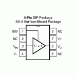
VIN is signal input on BUF634, or "IN" on the buffer module
VOUT is signal output on BUF634, or "OUT" on the buffer module.
You are correct that V+ & V- are correlating to the socket. GND is going to have to be connected elsewhere on the PCB. On the top of the Pimeta board, GND is that thick trace that runs along the caps, makes a turn and at the back of the pot, and up the middle towards the rows of resistors. You could connect to it anywhere but probably easiest is to use one of the existing holes that you aren't using for something else. Those holes would be either "IG", "IG2" or "PG", all of which are fairly near the POT which is near the signal ground which is suboptimal even if convenient.
Ideally you do not want to put the buffer ground point close to the signal input ground, rather placing it closer to the capacitors. If you were only going to use two electrolytic capacitors, I'd say put the GND at the last capacitor hole on that GND trace on top of the board. If you do use all 4 capacitor positions, I'd suggest you scrape off some of the lacquer on the trace right above the silkscreened word "Pimeta" on the board, and drill the holes for wires in the middle of that GND trace, then run the wires up from the bottom to solder into it. The other alternative would be to not cut off the electrolytic C2 and C3 capacitor leads very short, instead leaving a bit sticking out on the bottom of the PCB that you can solder wires onto to run to the buffer. If you did that just make sure you use the GND, not V+ or V-, cap leads.
If you want to use that tubing, put it on the other wires instead of the GND, IF you connect only one end of the outer braid to GND on the Pimeta board. I should elaborate that when I speak of GND now or previously I mean signal and virtual ground, trace and holes described previously.
If your case is metal, try without the tubing just make the metal case connected to GND via the jack mounts. I presume you are aware you don't want power V- input or headphone output GND connected to a metal case too.
If your case is metal, try without the tubing just make the metal case connected to GND via the jack mounts. I presume you are aware you don't want power V- input or headphone output GND connected to a metal case too.
- Status
- This old topic is closed. If you want to reopen this topic, contact a moderator using the "Report Post" button.