Hi there guys,
Got an Audison SR1Dk which outputs no High-side gate drive.
The driver boards has a very clean input and a very clean low-side output drive wave, but absolutely no High-side output wave.
I changed both HCPL3180 optocouplers, changed the LM219 comparator, changed the SMBTA92 (2D transistor) and checked every single resistor on the board. Everything is original RS-online material.
Anybody got an idea?
Attachments
I'm having difficulties finding the problem.
(See datasheet attached).
AD2K driver board pin 7 (VB mark) should be the Vcc voltage supply of the optocoupler.
Pin 9 (VSD mark) should be the Vee of the optocoupler
I once had a good working Audison SR1Dk and I measured the driver boards pins. Noted them in a word file.
Pin 7: +-11.63v DC with an output block wave on the oscilloscope.
Pin 9: +-3.11v DC with an output block wave on the oscilloscope.
The potential DC difference between these pins should be the 15v supply of the optocoupler.
There currently is no measurable waves present and also no DC voltage.
I can't conclude how the "VB mark" should get around 11.6v according to the datasheet. Since the "VCC mark" voltage is not present because of the output fets are not being installed.
Does anyone has an idea?
Attachments
Last edited:
Thanks for the explaination!
Ok, understood")
When connecting a speaker load to the terminal it should have a reference. But in this case there also won't be any voltage present on pin 7, 8 and 9 I suppose.
Am I correct to say that the supply voltage of the optocoupler of the high side is delivered by the "+VCC mark"?
If so, how can this circuit be checked and measured when only the output fets are connected with the "+VCC mark".
Since this amplifier does not accept output fets yet.
This amplifier should draw 1.51A idle on 12v PS voltage.
It currently draws 1.01A idle on 12V PS voltage.
Ok, understood
When connecting a speaker load to the terminal it should have a reference. But in this case there also won't be any voltage present on pin 7, 8 and 9 I suppose.
Am I correct to say that the supply voltage of the optocoupler of the high side is delivered by the "+VCC mark"?
If so, how can this circuit be checked and measured when only the output fets are connected with the "+VCC mark".
Since this amplifier does not accept output fets yet.
This amplifier should draw 1.51A idle on 12v PS voltage.
It currently draws 1.01A idle on 12V PS voltage.
Last edited:
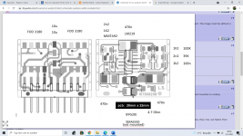
The optocouplers are not present on the schematics. The driver board schematics are not included.
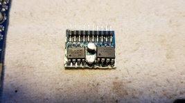
The High-Side optocoupler is present on the AD2K driver board.
In the beginning of this post is a photo from the driver board. The HCPL3180 IC on the right side is the one i'm reffering to.
Attached is the schematics from the driver board which I got from another DIYaudio post.
In this photo, the left HCPL3180 is the one i'm reffering to.
Attachments
Correct!!
On both High and Low-side bank of the output fets gate is now a square wave when there is a music signal.
If it's not the optocoupler..... What could it be...
Output fet gate drive is present.
Output filter inductor is mounted rock solid onto the board. I would not suspect it to be shorted. I will check it now
Last edited:
- Home
- General Interest
- Car Audio
- Audison SR1Dk output driver card, no High-side output