Hello to the fine people of the diyAudio forum. This is the second time I've written this post as the forum logged me out while I was writing the first.
I need assistance with an amplifier a friend asked me to look at. I am not a technician, electronics is a hobby that I am learning and am clearly out of my depth here.
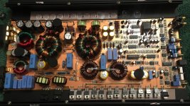
I am told it was being run hard, the supply voltage dropped and some magic smoke escaped. It appears to have had the output section repaired in the past but other than that I really have no info on its history.
The only visual clues I have are scorched gate resistors in the power supply with moderate damage to the top side of the board. The board is not conductive and the resistors all measure about 47 ohms.
I am powering the amp with a small, adjustable bench top supply with the current limited to 3 amps.
I have not fed the amp an audio signal.
Symptoms:
Power Supply:
Upon applying voltage to the remote terminal one of the transformers emits an audible, high frequency buzz for a second or two (I assume while the rail caps charge) then appears to operate normally. This behavior is at about 9.5 to 11.9 volts.
If I increase the supply voltage to 12-14 the transformer buzz returns and the PS FETs start heating up until I lower the voltage.
At the lower supply voltage the gates have a nice square drive wave. As the supply voltage is increased the duty cycle of the drive signal decreases. At 12v, I can only describe the drive signal as zero, it's no longer a square wave and continues to distort as the supply voltage increases.
I removed all of the PS FETs and tested them in a breadboard with a 10k potentiometer, 1k current limiting resistor and an LED and they appear to be operating correctly. I did this because the heat sink and clamps show signs of multiple failures but all the FETs passed the multimeter test. It is possible the scorch marks and soot are from a previous failure and were not cleaned up.
There appears to be no resistor between pins 5 & 7 of the SG3525A for setting the dead time. I do not know if this is relevant.
Output Section: (may not have a problem)
When probing the gates of the output FETs: both high side banks have a clear square drive signal; the low side banks have what appears to be 2 square waves, one 108 degrees out of phase with the other. Is this perhaps an issue with my trigger setting? When measured at the HIP4080 all four drive pins have a very clear square wave. The only components between the 4080 and the FETs are a pair of parallel resistors and diodes, one set for each bank and my meter does not show any problems without removing any components from their circuit.
The output FETs do not get hot.
During operation, the 4080 gets mildly warm (nowhere near hot,) is this normal operation?
There is no DC offset at the speaker output terminals, each terminal reads ~31 volts referenced to battery ground.
The rail capacitors discharge from ~60v to near 0 in about 30 seconds, is this normal behavior? I ask because I've read so many warnings about discharging the caps before working on the board.
If anyone could point me in the right direction I would very much appreciate it and will do my best to answer any questions you have. I have included all of the details I can think of and apologize for any that may be irrelevant. I do have a copy of Perry's guide and have read about 90% of it so far. It's very humbling to read as I don't know that much information about any 3 subjects combined.
Thanks for your consideration and patience.
I need assistance with an amplifier a friend asked me to look at. I am not a technician, electronics is a hobby that I am learning and am clearly out of my depth here.
I am told it was being run hard, the supply voltage dropped and some magic smoke escaped. It appears to have had the output section repaired in the past but other than that I really have no info on its history.
The only visual clues I have are scorched gate resistors in the power supply with moderate damage to the top side of the board. The board is not conductive and the resistors all measure about 47 ohms.
I am powering the amp with a small, adjustable bench top supply with the current limited to 3 amps.
I have not fed the amp an audio signal.
Symptoms:
Power Supply:
Upon applying voltage to the remote terminal one of the transformers emits an audible, high frequency buzz for a second or two (I assume while the rail caps charge) then appears to operate normally. This behavior is at about 9.5 to 11.9 volts.
If I increase the supply voltage to 12-14 the transformer buzz returns and the PS FETs start heating up until I lower the voltage.
At the lower supply voltage the gates have a nice square drive wave. As the supply voltage is increased the duty cycle of the drive signal decreases. At 12v, I can only describe the drive signal as zero, it's no longer a square wave and continues to distort as the supply voltage increases.
I removed all of the PS FETs and tested them in a breadboard with a 10k potentiometer, 1k current limiting resistor and an LED and they appear to be operating correctly. I did this because the heat sink and clamps show signs of multiple failures but all the FETs passed the multimeter test. It is possible the scorch marks and soot are from a previous failure and were not cleaned up.
There appears to be no resistor between pins 5 & 7 of the SG3525A for setting the dead time. I do not know if this is relevant.
Output Section: (may not have a problem)
When probing the gates of the output FETs: both high side banks have a clear square drive signal; the low side banks have what appears to be 2 square waves, one 108 degrees out of phase with the other. Is this perhaps an issue with my trigger setting? When measured at the HIP4080 all four drive pins have a very clear square wave. The only components between the 4080 and the FETs are a pair of parallel resistors and diodes, one set for each bank and my meter does not show any problems without removing any components from their circuit.
The output FETs do not get hot.
During operation, the 4080 gets mildly warm (nowhere near hot,) is this normal operation?
There is no DC offset at the speaker output terminals, each terminal reads ~31 volts referenced to battery ground.
The rail capacitors discharge from ~60v to near 0 in about 30 seconds, is this normal behavior? I ask because I've read so many warnings about discharging the caps before working on the board.
If anyone could point me in the right direction I would very much appreciate it and will do my best to answer any questions you have. I have included all of the details I can think of and apologize for any that may be irrelevant. I do have a copy of Perry's guide and have read about 90% of it so far. It's very humbling to read as I don't know that much information about any 3 subjects combined.
Thanks for your consideration and patience.
Last edited:
It just occurred to me that a picture of the board may be helpful but I can no longer edit my initial post. Please forgive the fact that it's backwards in the heat sink and the PS FETS are missing. The board is safer in the sink thank out when I'm not working on it.
Attachments
If you read an open connection between the gate and the other legs of the PS FETs, the FETs were likely replaced in a previous repair. The gate resistors won't burn otherwise.
I've tried the 3525 without a DT resistor and it would not oscillate. What's the resistance between 5 and 7?
Why are the outputs out of the amp/
The rail caps, in some amps, have bleeder resistors which drain the voltage. Some do not and in class D amps, without the bleeder resistors, the rail caps can remain charged for weeks. For those amps, you must discharge the rail caps. Even with bleeder resistors, you need to wait for the caps to drain (or manually drain them) before you work on it.
I appear to have made a mistake.
In circuit the PS FETs read 15 M ohms between the gate and other 2 legs with the black probe on the gate. With the red probe on the gate I'm reading 730k between the gate and other 2 legs. What a blunder...
The 3525 has no resistance between pins 5 and 7. Despite messing up my initial test of the PS FETs I am certain on this after double checking the data sheet to make sure I'm counting pins correctly.
The outputs are in the amp, I have not removed any of them. The FETs missing in the picture are the PS FETs.
Thank you for the clarification on the rail caps.
OK, I will pull the PS FETs back out tomorrow when my hands are steady enough to run the iron and check them properly. Is it safe to assume the driver transistors must be checked in the same fashion?
Yes sir, a direct short between pins 5 and 7. Glad to know that's OK.
That's OK I have the regular kind, hence the name Dsy.
Thank you so much for your guidance thus far, I will report back tomorrow with my findings!
EDIT:
I answered my own question about the driver transistors by re-reading "Checking Semiconductors" section. To check for leakage they must be removed from the circuit.
Last edited:
The drivers can generally be determined to be OK if the drive signal is good at the FETs.
You can probably just pull and check one FET for leakage. Then reinstall it and confirm that all of the other FETs have the same drive signal on the gate leg of the FET (not on the driver side of the gate resistor)
You can probably just pull and check one FET for leakage. Then reinstall it and confirm that all of the other FETs have the same drive signal on the gate leg of the FET (not on the driver side of the gate resistor)
OK, I pulled one PS FET and it reads an open circuit between the gate and other 2 legs with my leads in either polarity.
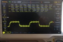
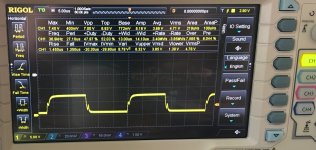
Attached is a picture of the drive wave measured at the gate, the amp is powered with 10v. All 12 gates look to have an identical signal, I can upload 12 pictures if needed. There is some noise in the signal, I'm not sure if it's from my cheap power supply or if there's an issue with the drive signal.
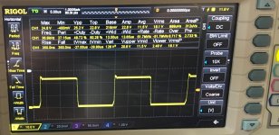
The second picture is what the drive wave looks like when it reduces to a duty cycle of "zero"? as I increase the voltage from my power supply and the transformer starts buzzing.
Attached is a picture of the drive wave measured at the gate, the amp is powered with 10v. All 12 gates look to have an identical signal, I can upload 12 pictures if needed. There is some noise in the signal, I'm not sure if it's from my cheap power supply or if there's an issue with the drive signal.
The second picture is what the drive wave looks like when it reduces to a duty cycle of "zero"? as I increase the voltage from my power supply and the transformer starts buzzing.
Attachments
What's the resistance between the source leg and the primary ground terminal? 0 ohms?
The issue is that it's not 0 ohms impedance to high frequencies.
There should be no inductor in series between the source legs and ground.
It's not safe to ground the scope to all source legs but on a push-pull switching power supply, it's safe (except the MTX types that use a gate drive transformer and 'follower' type drive for the transformer).
The resistance measures 0.1 ohms (the same as my leads shorted together.)
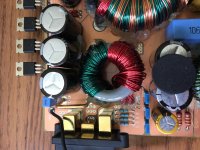
The inductor I referenced is pictured below. Perhaps "inductor" is not the correct term.
EDIT:
This is the waveform with the scope connected as per instructed.
The inductor I referenced is pictured below. Perhaps "inductor" is not the correct term.
EDIT:
This is the waveform with the scope connected as per instructed.
Attachments
Last edited:
Inductor is right but those are very rare. Well, technically, I think it's more correct to use choke instead of inductor for DC applications.
This is a common-mode choke. They are used in some of the high-end amps like Phoenix Gold but you don't see them on the DC input side of many amps.
This is a common-mode choke. They are used in some of the high-end amps like Phoenix Gold but you don't see them on the DC input side of many amps.
Ah yes, choke would have been a much better word choice. My apologies.
I included the waveform you requested in the above post, perhaps I shouldn't have edited it in. Being new here I'm not familiar how much double posts are frowned upon.
As you explained, it looks much cleaner with the scope connected correctly.
I included the waveform you requested in the above post, perhaps I shouldn't have edited it in. Being new here I'm not familiar how much double posts are frowned upon.
As you explained, it looks much cleaner with the scope connected correctly.
Double posts are bad but posting the photo twice would have been OK.
When I see a new post for a thread (bold text), I only use the green arrow to go to the last post (almost without exception so it's good to mention if you made edits or multiple posts.
The waveforms look different from 10-13v because the rail voltage is regulated (something else that's relatively rare in amps like this unless the rail voltage is near the upper limits for the output stage driver IC).
Understood, the last thing I want to do is irritate anyone kind enough to help.
Do you know why the transformer closer to the battery terminals starts buzzing when the supply voltage is increased above 12 volts?
Other than scorched gate resistors and noise from the transformer I don't see anything obviously wrong.
Do you know why the transformer closer to the battery terminals starts buzzing when the supply voltage is increased above 12 volts?
Other than scorched gate resistors and noise from the transformer I don't see anything obviously wrong.
The regulator circuit may not be perfect. The circuit needs to be fast enough to prevent voltage drop but not so fast that it's noisy. This one may not be damped enough to be quiet. When the amp is producing audio, the pulse width won't likely get down to where you saw it at 13v.
Sometimes, transformer noise is due to loose windings and moving them slightly will quiet them.
Sometimes, transformer noise is due to loose windings and moving them slightly will quiet them.
Interesting. I suppose I need to look into the regulation circuit.
The transformers are held down solid with silicon and the windings are held together with what appears to be epoxy. I can't get any of it to budge. No amount of pressure quiets it down.
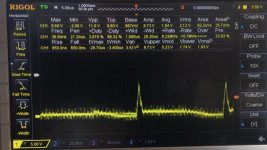
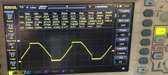
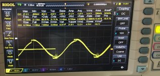
While I'm asking questions, these are the waveforms on the drain at 11.4v, 12.6v and 13.5v. Does this look abnormal for a regulated power supply? (13.5v has transformer noise, the others do not.)
The transformers are held down solid with silicon and the windings are held together with what appears to be epoxy. I can't get any of it to budge. No amount of pressure quiets it down.
While I'm asking questions, these are the waveforms on the drain at 11.4v, 12.6v and 13.5v. Does this look abnormal for a regulated power supply? (13.5v has transformer noise, the others do not.)
Attachments
- Status
- This old topic is closed. If you want to reopen this topic, contact a moderator using the "Report Post" button.
- Home
- General Interest
- Car Audio
- HIP4080 based amp repair help