The rectifiers need to be removed to allow more definitive testing of the drive circuit. The rail voltage doesn't need to be present and adds risk to the components as well as the scope if it's improperly grounded when testing.
Dear Perry,
Based on your latest post, I understand finally your point - you've got a good reason.
A. I am delaying the pulling of rectifiers for the rails due I've pulled already all IRF640 some days before - to check them properly one by one - I've wrongly suspected a failure among them that time - so , in that stage I had everything powered less the outputs (not onboard anymore) but ,
talking here with you I understand that IRF 640's gates work somehow as a "load" for drivers , and furthermore please correct me , maybe I'm wrong in understanding:
_"MODU1" act as a driver (pulse generator) and Q11,Q13,Q15 module is some kind of bipolar preamplifier, therefore we can check the signal directly on Q11,Q13,Q15 module input (where is O - correct) / output (where is steady 15V DC - wrong !) - no matter IRF 640's gate connected or not as a "load" , 15V all the time !
_when IRF 640 were connected it was +70V DC on speaker rail due that 15V DC permanent on Q11,Q13,Q15 module's output
B. Now , because you have a full picture , pls kindly direct your attention if I pull the rectifiers for the rails:
Scenario : We will have no more ± 80V on main rails, we will have outputs gates acting as load for Q11,Q13,Q15 module but
Prediction: we will have again 15V DC permanent on Q11,Q13,Q15 module's output, I can bet.
I think , if you agree , that the problem is in "MODU1" lined-up with Q11,Q13,Q15 module , linkage that generates that bloody 15 V DC.
I will revert with updates pending on:
_if Q11,Q13,Q15 module input grounded (strap between Q15 base-emitter - here is safe to strap) will make no change and still have 15 V on output, the fault is not in "MODU1" but in Q11,Q13,Q15 module as a DC polarisation problem - so, no reason yet to remove the rectifiers for a "simple" DC situation. Note: It is not simple due I can not explain from where 15 V ...
_if Q11,Q13,Q15 module input grounded (strap between Q15 base-emitter) will make a change and no more 15 V on output, the fault is in "MODU1" itself due Q11,Q13,Q15 module acts in this case only as a good bipolar preamplifier - BUT I can bet is no chance for this scenario due we have OV DC in this point and 15 V DC on Q15' collector - as marked in red before.
C. I don't have a schematic of "MODU1" to develop more scenarios - pls kindly provide some info regarding "MODU1" shielded box because you are the "class-D-amplifier-expert"
I wait for your kind answer and no , still do not have the scope.
I still hope to solve it with your help without a scope - for the moment we haven't passed the 15 DC issues here.
D. Can I use my laptop/soundcard as a primitive scope , I am aware that everything will be limited on 5V soundcard input restriction but at least will provide some info regarding sinusoidal curves - on next steps ?
I do not lie to you, I haven't yet use a scope since I've graduated my master's degree in maritime electronics, 20 years ago. Since then I've succesfully passed a lot of service situations in electronics - all kinds of them - but this amp stuck me and I need your help and if you say so, maybe I need a scope.
As I said, is 1st time I faced this situation of class D driver and I'm positive is something I am missing on the Sinuslive diagram ...
Last edited:
hi mr sed, that 15v on the gates, MIGHT be a problem, but flipside it could also NOT be a problem, i have seen some amps that drive in this manner with output fets removed, the safest way to check is to load 1 fet per bank and read the sine wave.
Dear Azeem,
already load few days before 1 fet per bank (you can see in pictures traces of resoldering of one from 4 fets) and having 15V DC on gate (MOS_DRV_H) and 70V on speaker rail.
I don't have yet a scope to check if only 15 V pure Dc is there but here is sure a problem.
With audio inputs grounded should be 0 due 15V will trigger the gate.
Last edited:
There is any way to audio-trace the audio signal processed in class D drivers / preamplifiers ? Like demodulating into audio spectrum ? I've tried to trace the signal from RCA input till .... end speaker rail and there is no audio signal / no audio modulation since 1st input capacitors...
No , guys , I will fabricate a scope tommorrow , I hope, somehow.
Till then , pls help me regarding: U4-6n137 - HIGH SPEED-10 MBit/s LOGIC GATE OPTOCOUPLERS - can I find it in some old switching supplies or anything like etc ? due it will take too long an online order.
A. Here I think is the problem and for whom it may concerns the normal idle state for Q15 or Q16 input transistors is HIGH and not low - nobody helped me in this matter !!! - automatically when the input is HIGH the transistor will ground the DC signal between E-C, therefore for Q11,Q13 or Q12,Q14 couples the output will be low and no more DC on outputs gates or speaker rail !!!!
I traced the DC signal all-around and found that on L block base of Q15 is high and that was correct (pin no.6 of U5 is HIGH). It is HIGH from pin no6 till base of Q15 - everything ok in L block.
I traced the DC signal in H block and found that on U4, pin no.6 , signal is LOW !!!
R68 is ok , therefore U4 might be fault.
Also , as a test, I made HIGH the base of Q15, R59,R58 and all H block ceased to have a HIGH output.
I don't know exactly how , but U4 seems defective altough it is not a power part, I think is a low power circuit , anyway here is the problem.
I will use a scope after I will correct the DC problem first or maybe I will need no more further.
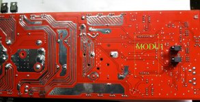
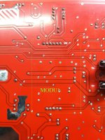
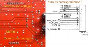
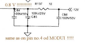
B. Does anybody know the pinouts for MODU1 ? ALSO HERE I detect a problem , see attached pinouts voltages , is missing -12 V , there is +12 V (10.11 V - I used a 10.9 V power supply) ...
Maybe -12V is on shielded upper part of MODU1 ?.. There is any diagram / schematic for MODU1 ?...
Many thanks
Till then , pls help me regarding: U4-6n137 - HIGH SPEED-10 MBit/s LOGIC GATE OPTOCOUPLERS - can I find it in some old switching supplies or anything like etc ? due it will take too long an online order.
A. Here I think is the problem and for whom it may concerns the normal idle state for Q15 or Q16 input transistors is HIGH and not low - nobody helped me in this matter !!! - automatically when the input is HIGH the transistor will ground the DC signal between E-C, therefore for Q11,Q13 or Q12,Q14 couples the output will be low and no more DC on outputs gates or speaker rail !!!!
I traced the DC signal all-around and found that on L block base of Q15 is high and that was correct (pin no.6 of U5 is HIGH). It is HIGH from pin no6 till base of Q15 - everything ok in L block.
I traced the DC signal in H block and found that on U4, pin no.6 , signal is LOW !!!
R68 is ok , therefore U4 might be fault.
Also , as a test, I made HIGH the base of Q15, R59,R58 and all H block ceased to have a HIGH output.
I don't know exactly how , but U4 seems defective altough it is not a power part, I think is a low power circuit , anyway here is the problem.
I will use a scope after I will correct the DC problem first or maybe I will need no more further.
B. Does anybody know the pinouts for MODU1 ? ALSO HERE I detect a problem , see attached pinouts voltages , is missing -12 V , there is +12 V (10.11 V - I used a 10.9 V power supply) ...
Maybe -12V is on shielded upper part of MODU1 ?.. There is any diagram / schematic for MODU1 ?...
Many thanks
Attachments
-
 sinuslive_2019-07-23-general bootom view.jpeg240.1 KB · Views: 70
 -
 sinuslive_2019-07-23-H block-problem.jpeg101.1 KB · Views: 66
 -
 sinuslive_2019-07-23-L block.jpeg97.7 KB · Views: 74
 -
 sinuslive_2019-07-23-MODU1 DC voltages.jpeg62.6 KB · Views: 62
 -
 sinuslive_2019-07-23-shielded bootom view.jpeg198.7 KB · Views: 70
Last edited:
Unfortunately the tests you have done are of little use if you don't have an oscilloscope.No , guys , I will fabricate a scope tommorrow , I hope, somehow.
Till then , pls help me regarding: U4-6n137 - HIGH SPEED-10 MBit/s LOGIC GATE OPTOCOUPLERS - can I find it in some old switching supplies or anything like etc ? due it will take too long an online order.
A. Here I think is the problem and for whom it may concerns the normal idle state for Q15 or Q16 input transistors is HIGH and not low - nobody helped me in this matter !!! - automatically when the input is HIGH the transistor will ground the DC signal between E-C, therefore for Q11,Q13 or Q12,Q14 couples the output will be low and no more DC on outputs gates or speaker rail !!!!
I traced the DC signal all-around and found that on L block base of Q15 is high and that was correct (pin no.6 of U5 is HIGH). It is HIGH from pin no6 till base of Q15 - everything ok in L block.
I traced the DC signal in H block and found that on U4, pin no.6 , signal is LOW !!!
R68 is ok , therefore U4 might be fault.
Also , as a test, I made HIGH the base of Q15, R59,R58 and all H block ceased to have a HIGH output.
I don't know exactly how , but U4 seems defective altough it is not a power part, I think is a low power circuit , anyway here is the problem.
I will use a scope after I will correct the DC problem first or maybe I will need no more further.
B. Does anybody know the pinouts for MODU1 ? ALSO HERE I detect a problem , see attached pinouts voltages , is missing -12 V , there is +12 V (10.11 V - I used a 10.9 V power supply) ...
Maybe -12V is on shielded upper part of MODU1 ?.. There is any diagram / schematic for MODU1 ?...
Many thanks
Very often, with the DMM you can make some measurements, but there comes the point where you need to see some things on the oscilloscope screen, only thanks to this you can understand if some fundamental parts of the amplifier work.
Of course, with DMM you can control working voltages, if they are present and if they are correct, but for the waveforms (often at very high frequency) how do you do it?
For example, now you need to figure out if the MODU works fine, and to do this you should check at its outputs if you see a square waveform (injecting a strong 100hz signal at the input) of the same frequency as the injected signal.
Then you can go to the next step.
I have done many repairs without an oscilloscope, but since I bought it, a new world has opened up and I have been able to do repairs that were too complex or impossible for me before.
Obviously it must be an investment that is repaid in the future with time. But if you do a repair every once in a while, maybe it's not worth buying one.
Thanks, you have right. I will Turn My Laptop Into an Oscilloscope, I know there will be limits but it will help.
For the moment I have this problems:
a) I bought in the morning a 6n137.
Driving my car I was wondering if really U4-6n137 is the problem due low output could be a defective optocupler but also could be a defective input for optocupler and the input is MODU1.
b) I have no diagram for MODU1, I've asked for , no reply. At least I would try to find it out somehow based on generic diagrams.
c) For SinusLive A1500 I have no pinouts of MODU1. I wonder if supply voltages are correct. Couldn't find -12 V pin due MODU1 is thoroughly shielded.
d) I don't know how to safe dismantle MODU1 to gain any acces to components, to check voltages. I tried the supposed soldering points but it doesn't move. It's a multilayer PCB and what is shielded give no acces.
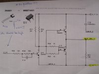
If you are patient, I will try to help you with the MODU pinout, but be sure that it is difficult to damage MODU because it is separated from the power section through the optocouplers (if you look at the internal diagram of the optocouplers in their datasheet, you will see that there is no it is electrical connection between the LED and the TRANSISTOR) therefore, if absurdly the power section explodes, the drivers (2n4401 and 2n4403) or the gate resistors, or the photo-couplers (transistors side), may break to the maximum, but at 99.9 % of cases, MODU will always be safe.Thanks, you have right. I will Turn My Laptop Into an Oscilloscope, I know there will be limits but it will help.
For the moment I have this problems:
a) I bought in the morning a 6n137.
Driving my car I was wondering if really U4-6n137 is the problem due low output could be a defective optocupler but also could be a defective input for optocupler and the input is MODU1.
b) I have no diagram for MODU1, I've asked for , no reply. At least I would try to find it out somehow based on generic diagrams.
c) For SinusLive A1500 I have no pinouts of MODU1. I wonder if supply voltages are correct. Couldn't find -12 V pin due MODU1 is thoroughly shielded.
d) I don't know how to safe dismantle MODU1 to gain any acces to components, to check voltages. I tried the supposed soldering points but it doesn't move. It's a multilayer PCB and what is shielded give no acces.
The only cases where MODU can break (based on my experiences) is due to a defect or excessive temperature.
Your opinion helps me a lot , I was just reading the datasheet for optocouplers now - before replacing one of them , trying to analise the chances to be MODU1 damaged or optocupler itself, damaged. As per your experience (MODU1 hard to be destroyed) and based on my DC tests (permanent low output of H optocupler) , the fault in my case should be optocupler ... I would replace it - hope to see some changes...
In my experience, there may be something after the optocoupler that could be damaged and could compromise your measurements at the optocoupler outputs.Your opinion helps me a lot , I was just reading the datasheet for optocouplers now - before replacing one of them , trying to analise the chances to be MODU1 damaged or optocupler itself, damaged. As per your experience (MODU1 hard to be destroyed) and based on my DC tests (permanent low output of H optocupler) , the fault in my case should be optocupler ... I would replace it - hope to see some changes...
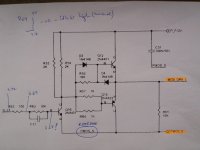
IMHO must remove the photo-couplers to be able to separate MODU from the rest, in this way you can control (with oscilloscope) if the inputs of the photo-couplers are the square wave (with a strong 100hz signal at the amplifier input).
Note that the inputs of the photo-couplers come directly from the MODU outputs, so if you find the correct wave, it is useless to go and look for the MODU outputs.
What happens before the optocouplers will let you know if MODU is ok.
What happens after the optocouplers won't tell you anything about MODU, so if there's a problem after the optocouplers, this is to be found in the photo-couplers and what's after them.
It seems to be faulty MODU1...
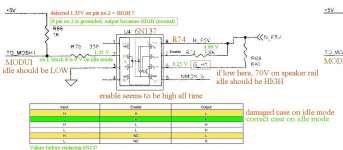
_6n137 reaction seems to be good, due 1.35V on its input can be considered HIGH comparative to block L, where on idle state it is 0V on input.
_if pin no. 2 grounded , output becomes HIGH (normal on idle state)
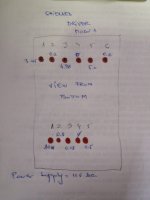
I desperately need the diagram or equivalent of it of MODU1 for SinusLive Sl-A1500 .. at least the pinouts on PCB... MODU1 is defective due wrong voltages (± 12V) or it's output is defective and I can not analise the reason (could be defective the input for MODU1 or MODU1 itself ) ...
_6n137 reaction seems to be good, due 1.35V on its input can be considered HIGH comparative to block L, where on idle state it is 0V on input.
_if pin no. 2 grounded , output becomes HIGH (normal on idle state)
I desperately need the diagram or equivalent of it of MODU1 for SinusLive Sl-A1500 .. at least the pinouts on PCB... MODU1 is defective due wrong voltages (± 12V) or it's output is defective and I can not analise the reason (could be defective the input for MODU1 or MODU1 itself ) ...
Attachments
In my experience, there may be something after the optocoupler that could be damaged and could compromise your measurements at the optocoupler outputs.
IMHO must remove the photo-couplers to be able to separate MODU from the rest, in this way you can control (with oscilloscope) if the inputs of the photo-couplers are the square wave (with a strong 100hz signal at the amplifier input).
Note that the inputs of the photo-couplers come directly from the MODU outputs, so if you find the correct wave, it is useless to go and look for the MODU outputs.
What happens before the optocouplers will let you know if MODU is ok.
What happens after the optocouplers won't tell you anything about MODU, so if there's a problem after the optocouplers, this is to be found in the photo-couplers and what's after them.
Pls check my findings... on block L seems to be everything ok, don't forget everything has begun due +70 V DC on speaker rail (due 15V on H outputs gates). I traced all signals from end to beginning ... till optocuplers ... and now I'm focused on MODU1 due on block H , on optocupler pin no.2 , is 1.35V DC permanent - on idle state. If grounded pin. no2 , the octocupler reacts fine, it's output became HIGH as should be on idle mode.
It is possible that -12V not to be supplied on MODU1, not found on measuring - see photo attached before (yesterday) with my handwriting. I will work to find correspondence between PCB and diagram regarding MODU1 pinouts ...
Attachments
Last edited:
Everyrhing seems to be ok now , only a problem : Q4 tested by voltmeter looks fine but back on board trigger the protection and in speaker is a weak noise of few hundrets Hertz.
Due is night and I have no spare IRF 640, I replaced Q4 by IRF540 (100V - 22A) instant burned (altough is only 80V on rail).
Amplifier works fine - not fully loaded - with only 3 outputs on block H (all outputs on block L onboard again) and outputs are cold on both blocks, H and L.
If connected IRF 740 (10A/400V) instead of Q4 the amplifier works fine but outputs temperature is increasing quickly and doesn't seem safe at all.
Any explanation ? Tommorrow I will buy a IRF640, I have all kinds of IRF in my workshop but 640 ...
Thank you, pls some more help...
A. Regarding pairing of MOS-FET , wich could be the cause the amplifier works "fine" with 1H+1L outputs, with 2H+2L outputs , ... , with 3H+4L outputs but will burn all times the Q4 output, if connected. PCB for Q4 and measurements looks fine for main board. Somehow all are paired in "parallel", so it's a matter of pairing.
B. I would like to reduce the "treble-middle cut" , meaning to add some more treble-middle due bass frequencies are too much but I don't guess very easy wich capacitor(s) are used for filtering .
One of them should be C95 , but should be more ...
Thks
Last edited:
- Status
- This old topic is closed. If you want to reopen this topic, contact a moderator using the "Report Post" button.
- Home
- General Interest
- Car Audio
- SinusLive SL-A1500 driver paradox