Please read the 'best initial settings' section on page 73 of my car audio site.
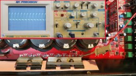
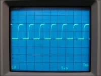
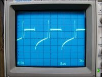
You have to center the trace before looking at the signal.
Use the ground position in the coupling switch to set the trace.
Use DC coupling when viewing/photographing the waveform.
Set the timebase so that you have about 3-4 cycles displayed.
Why are you questioning the signal you see?
You have to center the trace before looking at the signal.
Use the ground position in the coupling switch to set the trace.
Use DC coupling when viewing/photographing the waveform.
Set the timebase so that you have about 3-4 cycles displayed.
Why are you questioning the signal you see?
#3:
In some amps, they use a parallel resistor/diode to induce deadtime. I don't know if that's true for this amp.
joselorenzo :
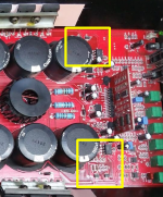
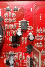
Can you post a couple of good quality photos (in focus, no flare from the flash...) of the areas indicated in the attached photo?
In some amps, they use a parallel resistor/diode to induce deadtime. I don't know if that's true for this amp.
joselorenzo :
Can you post a couple of good quality photos (in focus, no flare from the flash...) of the areas indicated in the attached photo?
Attachments
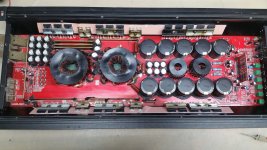
The amplifier I have tried to repair twice.
Now this last attempt changes
U9, U11, Q3, Q4, Q6, Q7, Q8 and Q9.
All IRFP260N are also new.
I have doubts with the waveform because I have no experience in this amplifier design
EDIT : I have problems uploading pictures
Now this last attempt changes
U9, U11, Q3, Q4, Q6, Q7, Q8 and Q9.
All IRFP260N are also new.
I have doubts with the waveform because I have no experience in this amplifier design
EDIT : I have problems uploading pictures
Attachments
Last edited:
I think I have a similar amp that I can repair to check the waveforms but if you get it repaired, post it so I don't have to fix that amp.
I'll wait until I can compare the waveforms by getting another similar amplifier or with help from you or some other forum member.
Any advance I do know
Thank you
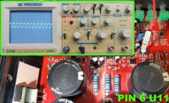
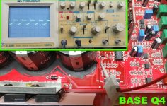
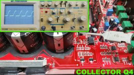
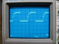
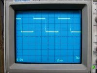
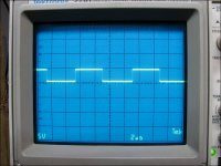
Note timebase and vertical amplifier setting for each.
Mouseover for descriptive file names.
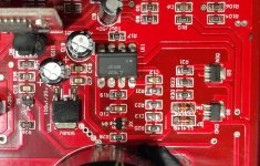
Q10 = Q4
Mouseover for descriptive file names.
Q10 = Q4
Attachments

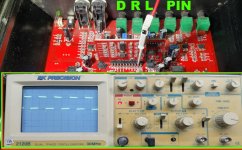
What do the base and emitter waveforms on the DK and the base of the AG transistors look like?
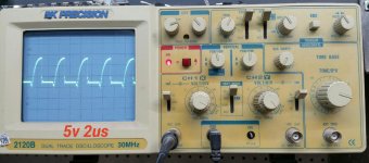
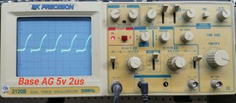
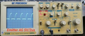
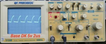
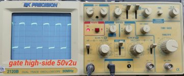
I upload pictures of the waveforms of DK and AG LOW SIDE AND HIGH SIDE.
Are you using the exact replacement outputs from a reputable distributor?
Verical and lcsc.com
What does the gate on the high-side look like?
I upload pictures
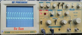
What's the timebase setting on your scope?
In all the recent measurements with photography Time/Div 2us
I upload pictures of the waveforms of DK and AG LOW SIDE AND HIGH SIDE.
Are you using the exact replacement outputs from a reputable distributor?
Verical and lcsc.com
What does the gate on the high-side look like?
I upload pictures
What's the timebase setting on your scope?
In all the recent measurements with photography Time/Div 2us
Attachments
Last edited:
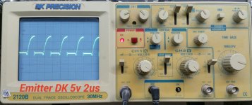
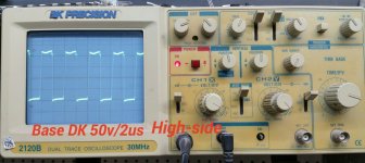
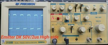
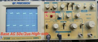
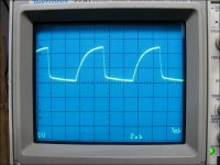
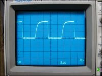
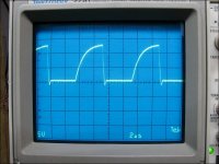
The following measurements with photography are from the AG and DK transistors on the high side
And the gate waveform output transitor
And the gate waveform output transitor
Attachments

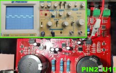
Is the var sweep control fully clockwise on your scope?
Unless you have two probes and you use your scope in differential mode with DC coupling, I think you're going to have to remove the rectifiers to get usable high side waveforms. The waveforms I posted that show the partial face of the scope were all taken with no rectifiers. These are the low side.
Q12 is the NPN driver. Q14 is the PNP driver. The emitters of both are directly connected so only one photo is needed.
Did you buy these FETs from verical or lcsc? I don't see lcsc as being authorized by any semiconductor manufacturer.
Attachments
Last edited:
- Status
- This old topic is closed. If you want to reopen this topic, contact a moderator using the "Report Post" button.
- Home
- General Interest
- Car Audio
- Rockseries 3000w gate output waveform