Hi,
Troubleshooting a Audio System X-330.2. It's A/B Mosfet-based 2ch car amplifier. It had two shorted output transistors (33N10 N-CH MOSFET) on the left side after being loaded with too low impedance according to the old owner.
The dead mosfets were shorted between gate-source-drain. I removed both and the amp started up so I went ahead and replaced all mosfets (5x N-CH) and (5xP-CH) so they were of the same batch. The amp started up fine, I tested the output with a signal generator and it looked fine at first glance.
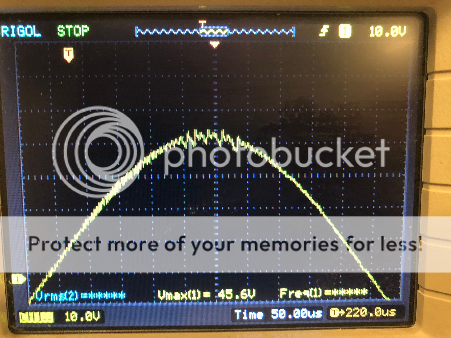
I then connected a speaker to test it under load and now the amp distorts heavily. Looking at the waveform the positive side collapses while the negative side looks fine. If you zoom in on the top part of the positive half of the waveform there are large amounts of ripple as you getting close to rail voltage, when the amp clips it starts drawing an abnormal amount of current (my lab supply goes into constant current).
After some additional troubleshooting I found the waveform and the distortion present on one of the pins of a 5532 opamp so I assumed it was there the distortion came from. I replaced that one too but still the same issue. There are a couple of BJT smd transistors and some form of bias circuitry around this area too, I've measured all the junctions and cannot find any issues. I compared the results to the functioning right side and nothing I've measured deviates.
*The output starts showing signs of ripple with as low load as 100 ohms and collapses completely with 5-6V on the positive side (looks a mess of random noise) and around 60V on the negative side of the sine wave.
*One of the mosfets I replaced (the exact same one that was shorted) heats up really fast once the ripple starts of appear on the output. I replaced the same mosfet again but still the same issue. Same mosfet heats up (N-CH) while all the others are of even temperature (fairly cold). Nothing else seems to get hot from what I can see.
-- Anyone have any idea what this could be? How does these types of amps work? The waveform is present on the drain but I only see DC on both source and gate. (same for the functioning side)
Here's how the ripple looks with an unloaded output (with small loads the bigger part of the waveform gets really "noisy"):
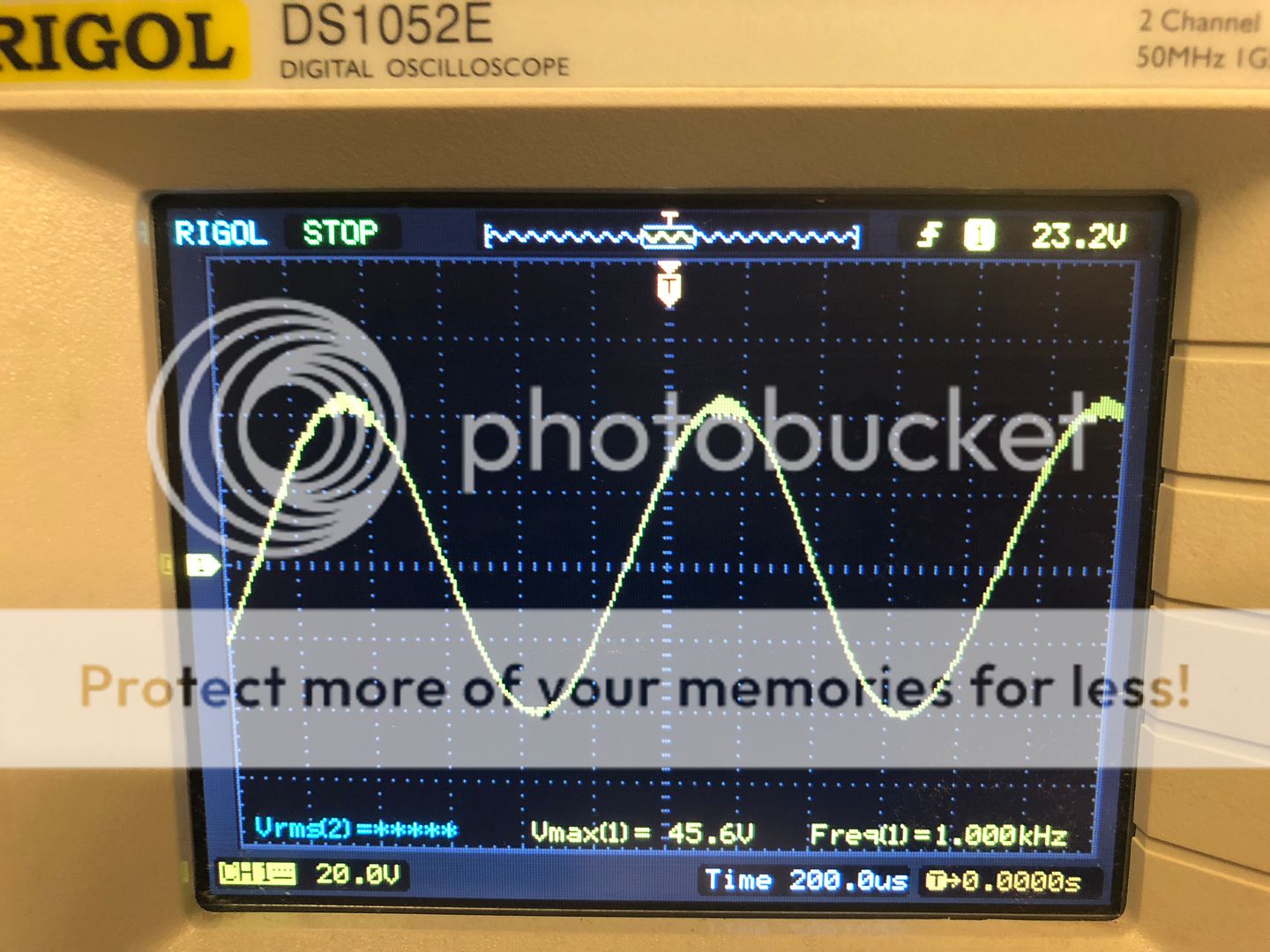
At clipping
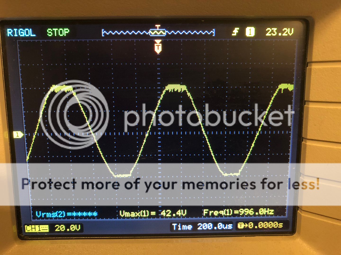
Zoomed in:
Troubleshooting a Audio System X-330.2. It's A/B Mosfet-based 2ch car amplifier. It had two shorted output transistors (33N10 N-CH MOSFET) on the left side after being loaded with too low impedance according to the old owner.
The dead mosfets were shorted between gate-source-drain. I removed both and the amp started up so I went ahead and replaced all mosfets (5x N-CH) and (5xP-CH) so they were of the same batch. The amp started up fine, I tested the output with a signal generator and it looked fine at first glance.
I then connected a speaker to test it under load and now the amp distorts heavily. Looking at the waveform the positive side collapses while the negative side looks fine. If you zoom in on the top part of the positive half of the waveform there are large amounts of ripple as you getting close to rail voltage, when the amp clips it starts drawing an abnormal amount of current (my lab supply goes into constant current).
After some additional troubleshooting I found the waveform and the distortion present on one of the pins of a 5532 opamp so I assumed it was there the distortion came from. I replaced that one too but still the same issue. There are a couple of BJT smd transistors and some form of bias circuitry around this area too, I've measured all the junctions and cannot find any issues. I compared the results to the functioning right side and nothing I've measured deviates.
*The output starts showing signs of ripple with as low load as 100 ohms and collapses completely with 5-6V on the positive side (looks a mess of random noise) and around 60V on the negative side of the sine wave.
*One of the mosfets I replaced (the exact same one that was shorted) heats up really fast once the ripple starts of appear on the output. I replaced the same mosfet again but still the same issue. Same mosfet heats up (N-CH) while all the others are of even temperature (fairly cold). Nothing else seems to get hot from what I can see.
-- Anyone have any idea what this could be? How does these types of amps work? The waveform is present on the drain but I only see DC on both source and gate. (same for the functioning side)
Here's how the ripple looks with an unloaded output (with small loads the bigger part of the waveform gets really "noisy"):

At clipping

Zoomed in:

Last edited:
When the output transistors go, especially when the gate goes short, it can damage components further back in the chain.
I would be replacing any drivers too.
I had an amp that didn't play right and all the transistors checked out ok.
It was only when I did an Hfe test did I find one transistor had an Hfe of 1 !
I would be replacing any drivers too.
I had an amp that didn't play right and all the transistors checked out ok.
It was only when I did an Hfe test did I find one transistor had an Hfe of 1 !
 moved to car audio forum.
Which terminal of the 5532 had noise?
Does the voltage on pins 4 and 8 remain constant, no matter the output signal distortion?
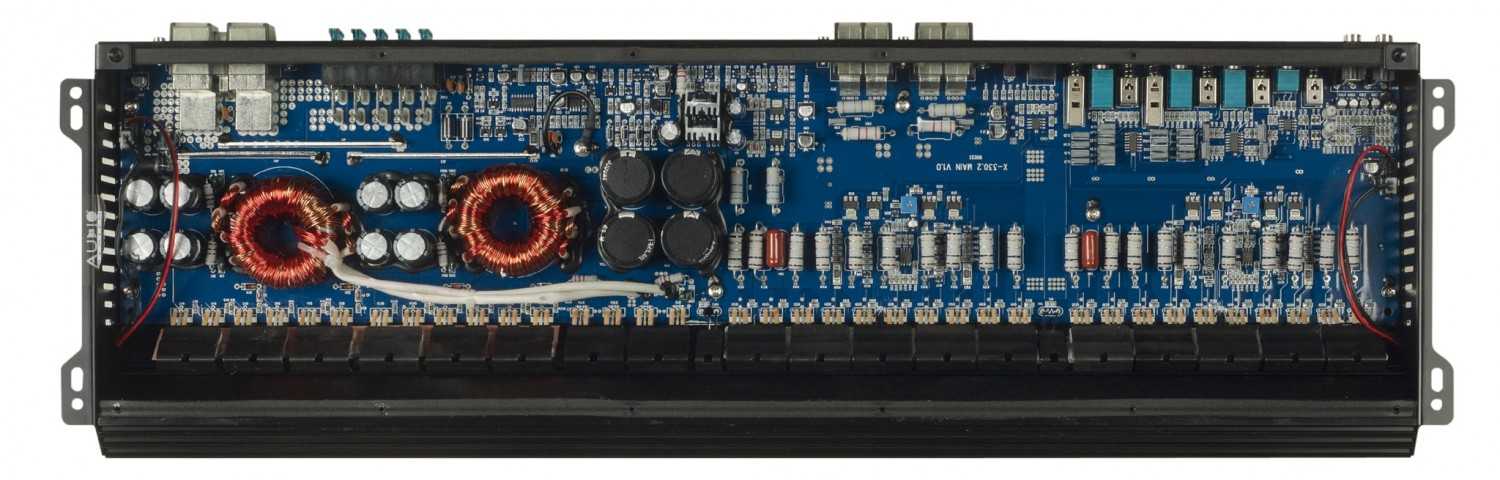
I don't know the amp you have but I think it's a larger version of the amp attached. Is the circuit similar?
Does the voltage on pins 4 and 8 remain constant, no matter the output signal distortion?
I don't know the amp you have but I think it's a larger version of the amp attached. Is the circuit similar?
Attachments
Last edited:
Ok. Here's some interesting things. When I measure Pin 4 and 8 of the functioning side I get:
6.68V and -6.24V
When I measure the faulty side the amp goes from 1A idle to 5A current draw and goes into protect within a second. That's with a battery powered DMM. Touching the surrounding active components give pretty much the same voltage readings as the functioning side but you definitely see that it increases it's current draw (this is all with no signal applied at all, at idle). I have the DMM ground at the negative power terminal to the amp.
Update: Found one thing. If I put the DMM ground lead the RCA input it doesn't go into protect. Current draw goes up from 1A to 1,5A and voltages at idle are about the same as the other side, slightly lower. If I put DMM ground lead at the ground power terminal it goes haywire again.
What's going on, it's lost ground reference or something?
Update 2: I measured with the oscilloscope and DMM at the same time and noticed the waveform was clean now. When I got the DMM connected between ground and pin8 of the NE5532 opamp the problems goes away. Waveform stays clean. At least at idle. IIRC my DMM got like 1Mohm impedance or something. It got to be a grounding issue somewhere right?
Last edited:
Hi, connect a 4.7ohm resistor in series to a 2.2nF polyester capacitor.Ok. Here's some interesting things. When I measure Pin 4 and 8 of the functioning side I get:
6.68V and -6.24V
When I measure the faulty side the amp goes from 1A idle to 5A current draw and goes into protect within a second. That's with a battery powered DMM. Touching the surrounding active components give pretty much the same voltage readings as the functioning side but you definitely see that it increases it's current draw (this is all with no signal applied at all, at idle). I have the DMM ground at the negative power terminal to the amp.
Update: Found one thing. If I put the DMM ground lead the RCA input it doesn't go into protect. Current draw goes up from 1A to 1,5A and voltages at idle are about the same as the other side, slightly lower. If I put DMM ground lead at the ground power terminal it goes haywire again.
What's going on, it's lost ground reference or something?
Update 2: I measured with the oscilloscope and DMM at the same time and noticed the waveform was clean now. When I got the DMM connected between ground and pin8 of the NE5532 opamp the problems goes away. Waveform stays clean. At least at idle. IIRC my DMM got like 1Mohm impedance or something. It got to be a grounding issue somewhere right?
Take this circuit you just made and connect it to the non-working channel output (resistor side to the output and condenser side to the center tap of rail capacitors) Now check if you have the same problem..
Hi, connect a 4.7ohm resistor in series to a 2.2nF polyester capacitor.
Take this circuit you just made and connect it to the non-working channel output (resistor side to the output and condenser side to the center tap of rail capacitors) Now check if you have the same problem..
Tried it, minor difference. The noise reduces slightly but the fault is still there.
However, if I touch the DMM probe on pin 8 on the OPamp without even having the ground lead connected it fixes the problem. Very weird. It must see some form of path to ground even if it's several hundreds Mohm, at least that's my theory.
Same thing happens if you touch random components around the area of the OPamp. I seriously don't get it.
Sorry, said pin8 - I meant pin4 Vcc- before.
Putting the 2,2nF + 4.7Ohm RC circuit between center tap of the rails and pin7 (2OUT) of the 5532 OPamp eliminates the distortion completely. Just touching the cable going to that pin eliminates the distortion. If you leave it hanging it mid air not connected to anything it exaggerates the problem and the entire positive side of the waveform goes fuzzy.
I think I've measured all components on this side of the board by now without finding anything out of the ordinary. Weird...
Update, I tried connecting a speaker now. Works fine till 7kHz then it starts drawing excessive current again and goes into protect. I have no idea what's going on with this amp.
When it begins drawing excessive current, which FETs are heating up?
Only 2 FETs are. The exact ones that I replaced (twice). The N-Ch fets (33N10), they are from a reputable seller and of the same batch.
I measured to find the transistors closest in the chain leading up to the gate and replaced both (BC860C PNP and a BC850 NPN). No change in behaviour.
Edit, with lower output I can run it without it running away. This looks like massive crossover distortion, problem in the bias circuitry perhaps? Don't mind the spikes, they are from my shitty signal generator which can't output clean sine waves at 0.1V.

Last edited:
With the bias pot set all the way to the right, it 'almost' removes the crossover distortion but now different transistors are heating up. After turning the bias pot the one other N-CH mosfet heats up and two P-CH fets.
After 10 sec driving a speaker at fairly low voltages I read these temperatures (degrees C)
30 - 31 - 31 - 37 - 31 // 29 - 29 - 42 - 30 - 31 (N-CH / P-CH). Before it was the first two N-CH fets that was heating up. During the first test one N-CH was heating up to nearly 90 degrees C with only a few seconds of that noisy clipped signal being amplified.
Again, this gotta be one of the more stranger issues I've dealt with.
Well, I put it together again. Seems to not overheat once mounted on the heatsink. However this "repaired" side got pretty high DC offset 0.405V vs 0.08 on the good side. I see higher 3rd order harmonics than I'd like too, it's nothing crazy but still. I think I'll leave this until I might get hold of a service manual or something.
Thanks for the help guys.
Thanks for the help guys.
Did you look at the manual I posted?
Yes, some parts look similar. I don't seem to have the dual diodes in series but it does use the BC860, BC850 transistor combo in a similar manner. The equivalent Q13 and Q15 transistors in my circuit doesn't seem to go to ground, there's a 47ohms resistance to ground at the power terminal from the collector of these two.
Don't understand the schematic fully. DD4, DD5 seems to go into nowhere for example, am I getting this right? Does the input signal really go to the drain of the output MOSFETs?
- Status
- This old topic is closed. If you want to reopen this topic, contact a moderator using the "Report Post" button.
- Home
- General Interest
- Car Audio
- Mosfet A/B amplifier troubleshooting - strange issue