I haven't had to repair many of the amps with this driver board but you should be able to remove the rectifiers to check the drive circuit with no risk the the outputs or drive components. You'll need to supply the high-side with supply voltage. A 9v battery works for that.
I don't know about the N-version but the N-generally only causes problems in non-switching amps (class AB, etc). The n-version is geared towards amps like this. Maybe someone has a more definitive answer.
I don't know about the N-version but the N-generally only causes problems in non-switching amps (class AB, etc). The n-version is geared towards amps like this. Maybe someone has a more definitive answer.
Well, I have it working again. I built some jumpers and got the driver board out of the amp where I could probe it. Since this amp has pulldown resistors on each gate I removed the 4R7 resistor that supplied the low side gates. The amp would then power up, but with about 11V refrenced to negative rail on the low side output of the driver. I started probing the driver board and found that there was no Vcc. I repaired a cracked solder joint and now we have Vcc and the low side gate supply is no longer being driven high. I reinstalled the 4R7 resistor and it is again producing audio, but it has another issue somewhere.
I thought to measure rail voltage before putting it back together. I wanted to ensure that the rail caps were rated correctly and ensure that my pick for schottky diode was going to be good enough. With no current limiting resistor in series the negative rail measures -56Vdc, the positive rail was at 96Vdc. This is a bit higher than the rail caps are rated for, and obviously they should not be this asymmetrical. I know I have seen unequal rails mentioned on here before, but I cannot recall where and what the suspected cause was. Can anyone offer some guidance?
Thank you!
Jason
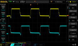
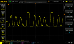
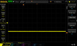
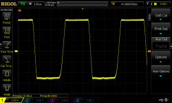
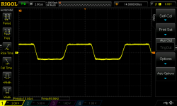
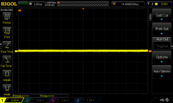
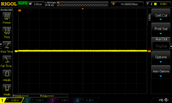
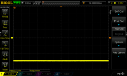
So, I have done some more testing this morning. I powered up the amp and took a look at the gate drive for the PS. Pictures are attached below. The first SS looks like there is nothing much unusual about the drive signal. So, I check the rails again and they are perfect, +/-60Vdc. I did not see anything out of the ordinary, so I started to think I may have misplaced my ground during testing. I began reassembling the amp and checked the PS after each set of transistors was clamped. No issues, rails were still symmetrical. Once I had it in the sink, I powered it up and was going to test under low power with a 6 ohm load.
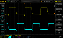
I hooked up the driver and then thought to check the rails again. Well, the went asymmetrical again, positive up near 100Vdc, negative at -55Vdc. I checked the gate drive again while there was a load (2nd two pics below), the gate drive looks perfect even while this is happening. I double checked that my reference was common to the secondary ground, it is. I checked the AC output of both transformers at the outer terminals of each rectifier and they are all 56Vac, I'm having trouble wrapping my head around this. With the load removed the rails go back to normal over a few seconds time, again, PS gate drive pulse width does not change.
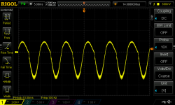
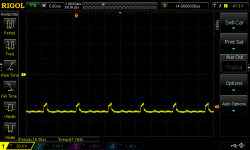
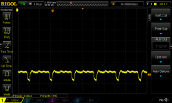
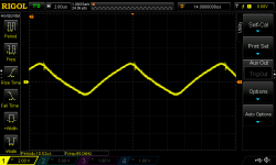
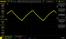
The last SS below shows the output of the amp. I was driving it with a function generator, .2Vp-p amplitude sine wave at 100Hz. I do not believe it should be offset so far, it's almost as if the high side is not the same amplitude, not merely just shifted downward. Also, with no speaker load hooked up the output of the amp looks like a sawtooth wave, I am guessing that is the result of the output filter not having the correct impedance present?
Thanks for taking the time to look it over.
Jason
I hooked up the driver and then thought to check the rails again. Well, the went asymmetrical again, positive up near 100Vdc, negative at -55Vdc. I checked the gate drive again while there was a load (2nd two pics below), the gate drive looks perfect even while this is happening. I double checked that my reference was common to the secondary ground, it is. I checked the AC output of both transformers at the outer terminals of each rectifier and they are all 56Vac, I'm having trouble wrapping my head around this. With the load removed the rails go back to normal over a few seconds time, again, PS gate drive pulse width does not change.
The last SS below shows the output of the amp. I was driving it with a function generator, .2Vp-p amplitude sine wave at 100Hz. I do not believe it should be offset so far, it's almost as if the high side is not the same amplitude, not merely just shifted downward. Also, with no speaker load hooked up the output of the amp looks like a sawtooth wave, I am guessing that is the result of the output filter not having the correct impedance present?
Thanks for taking the time to look it over.
Jason
Attachments
I feel like an idiot, I thought you were saying that the power supply drive was irregular. You are talking about the output drive. That does make sense, I'll check the drive signal on the outputs today. Will I need to pull the rectifiers and use a 9v for high side as recommended earlier, or can I check it as is since it is powering up with no protect or abnormal current draw?
Sorry for being so dense on this one, I think I was looking at things the wrong way.
Thanks,
Jason
Sorry for being so dense on this one, I think I was looking at things the wrong way.
Thanks,
Jason
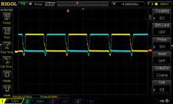
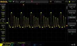
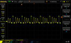
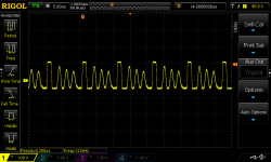
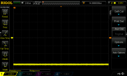
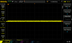
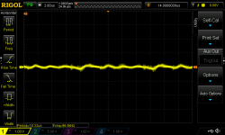
Ok, this is going to probably take a few posts due to the picture limit. The pictures are all named for where the waveforms were captured. For reference, I am calling the half bridge driver U1, the top TL072 U2 and the last TL072 U3.
Unfortunately the silkscreen designation is under the parts.
I tried to match the driver board waveforms to one of the larger ones I found in the tutorial, but things are not remotely similar, so either I have big problems, or this board is a fair bit different than it's larger brothers. I'm leaning toward it being "big problems"...
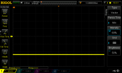
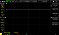
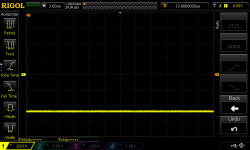
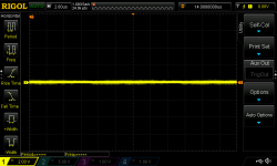
All waveforms were captured with the scope referenced to secondary ground. No input to the amp. All captures were with a 6ohm load connected. I got no drive pulse at all with no load on the amp.
Here are the output Fets first:
Unfortunately the silkscreen designation is under the parts.
I tried to match the driver board waveforms to one of the larger ones I found in the tutorial, but things are not remotely similar, so either I have big problems, or this board is a fair bit different than it's larger brothers. I'm leaning toward it being "big problems"...
All waveforms were captured with the scope referenced to secondary ground. No input to the amp. All captures were with a 6ohm load connected. I got no drive pulse at all with no load on the amp.
Here are the output Fets first:
Attachments
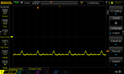

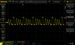
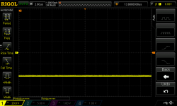
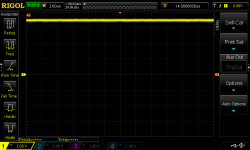
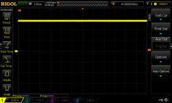
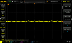
U2 (Top TL072):
It looks like this op-amp is only seeing +/-7Vdc rails, that can't be correct, can it?
It looks like this op-amp is only seeing +/-7Vdc rails, that can't be correct, can it?
Attachments


Last edited:
Quick update, I think it is fixed for real this time. Perry, when you said those driver ICs were sensitive, you meant it. This morning I removed all the ICs I replaced just to make sure the solder paste did not bridge anything under any of the chips. I was really grasping at straws. I cleaned the board again, reinstalled them and put it back in the amp. All the wave forms were the same except all of the sudden I lost all of the gate drive I had.
I checked the IC again per the previous instructions, and it was shorted. I removed it and put in the 3rd IC and voila! We have perfect square waves on the gates, with and without a load attached. I tested with the function generator and the distortion is gone. I will have to do burn in tomorrow, my back has had about all it can take for the day.
Thanks for the patience and for the assistance.
Jason
There is also a SMD diode missing from the driver board. The other one in the same package on the board is 639A, I searched high and low for that, and it looks like it might be a 18V zener transient surge suppressor. I would like confirmation if anyone has the info.
Thanks,
Jason
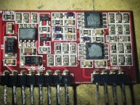
Just wanted to add a photo of the complete audio driver board for reference as I'm working on the same amp currently and the amp. The wierd thing about mine is it also had a shorted zenner going Into the driver board but when I sucked the solder out of the vias I found it was like they cut the leads and soldered into place or they just broke off inside the via which is a first for me.
Attachments
- Status
- This old topic is closed. If you want to reopen this topic, contact a moderator using the "Report Post" button.
- Home
- General Interest
- Car Audio
- DB drive OKUR A7 2000.1 driver