Thanks for the info in this thread - very helpful as I know very little about electronics.
I needed something to play classic rock type music and settled on a point to point silver wired DAC:
Jocko Homo/300_Baud input buffer (ble0t schematic fed with 5V) from another thread
Bobken Series Regulators (I think the J510 diode is the wrong way round in the schematic)keep compact!
CS8412 with .2uF/220R PLL and Analog ground separated from Digital Ground.
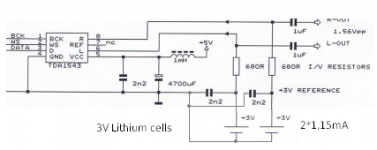
Single Tda1543 with pin 7 floating as per EC Designs in another thread
That gave a really nice clean sound - far too nice for my purposes.
So I finished off with 4.7 Obbligato MKP Coupling Caps. I then bypassed them with Kemet T140 67uF Axial Tantalum's - these add a nice bit of bass and just the right bit of distortion.
I needed something to play classic rock type music and settled on a point to point silver wired DAC:
Jocko Homo/300_Baud input buffer (ble0t schematic fed with 5V) from another thread
Bobken Series Regulators (I think the J510 diode is the wrong way round in the schematic)keep compact!
CS8412 with .2uF/220R PLL and Analog ground separated from Digital Ground.
Single Tda1543 with pin 7 floating as per EC Designs in another thread
That gave a really nice clean sound - far too nice for my purposes.
So I finished off with 4.7 Obbligato MKP Coupling Caps. I then bypassed them with Kemet T140 67uF Axial Tantalum's - these add a nice bit of bass and just the right bit of distortion.
I have a question if anyone is feeling nostalgic. I am building the original DAC at the start of this post. I am getting 11.5V instead of 8.3V for the DAC psu. I may not be interpreting the schematic correctly. I have rectified supply in through 15R with 2200uf bypass to BSP129 drain(4), gate(1) to source(3) bypassed with 15R and source out as pos circuit supply [CT neg/ground]. AD811 [2] + fed by 428R, 1 K to ground, AD811 [3] - fed by LM285-2.5 (2.5V out), 470R to +. AD811 [6] out to 470R to ZVN3310 gate, source to grnd/neg, drain to + bypassed by 10uf to voltage out. Power is AD811 [7] +, AD811 [4] - bypassed .1uf. And I get 11.5V not 8.3. I have the depletion mosfet at the input side of AD811, should it be at the output of the ZVN3310? Thanks for any help.
Steve
Steve
Hi Steve, here is the correct schematic:
Go over every single connection one more time, make sure there's no solder bridges or bad joints, every part is right way round etc. If in doubt, check the respective datasheets for pin-outs. You will get there eventually, just be patient and methodical")
An externally hosted image should be here but it was not working when we last tested it.
Go over every single connection one more time, make sure there's no solder bridges or bad joints, every part is right way round etc. If in doubt, check the respective datasheets for pin-outs. You will get there eventually, just be patient and methodical
Thanks for the info, I realized I mixed the 5 and 8.3V info in thread. Anyway I have the LMZ oriented as you show but I have it below the 470 as all the diagrams I find have it with ground then LMZ then resistor with 2.5V at junction. I am getting 2.5V to AD811 pin 3, is that correct. Also my datasheet say pin 6 is output of 2 and 3 so I have them first in the circuit a mirror of diagram right to left,is that wrong also?Thanks? Is there any info of voltages to check where? Will be playing with breadboard again!!!
Steve
Steve
Hello Steve,
The diagram shown in Uncle Leon’s post 304 is correct, so follow it carefully. This circuit was designed specifically to allow the use of an N channel mosfet for the regulator output stage. At the time of design N channel devices with the required operating parameters were much more common than P channel devices. This does require that the reference diode and its bias resistor are wired as shown in the diagram and not with their position swapped as would be required if using a P channel mosfet.
From your description of your regulator build you have not followed this circuit diagram. It appears that you have taken the current source output direct from the BSS129 source terminal instead of the other side of the 3R gate/source resistor. It will still behave as a current source but the current will settle at the IDSS of the BSS129. Also, from your description you appear to have swapped the position of the reference diode and it’s bias resistor. This will prevent the regulator from regulating correctly.
Nikonf2, the 3R resistor defines the current passing through the current source so it can be used to adjust the standing current in the shunt regulator section.
The AD811 is not specified for operation at 5vdc, however, if the input common mode voltage range and the output voltage swing range are both honoured in the design it will operate in this regulator circuit at 5vdc with reduced performance (although still way better than any of the common three terminal regulator options). The ZVN3310 gate to source voltage for a given drain current may be outside the output swing capability of the AD811 on a 5v supply so it is pertinent to check the gate source voltage requirement of this device over the full range of operating current of the regulator.
Regards
Paul
Hi Nikonf2,
Unfortunately the BSS129 is quite variable from device to device and batch to batch with respect to gate/source voltage verses operating current. You will have to work with this empirically by choosing a resistor value and measuring the voltage across the resistor. The current source current C (in Amps) will be V (volts across the resistor) divided by R (the resistance in ohms). Allow the circuit to thermally stabilise before taking a voltage reading. In the 5v regulator circuit allow 0.03A (30ma) for the AD811 quiescent current, operating headroom, the vref bias current and feedback resistor static current draw. The rest of the current available from the current source will be available to the load.
The BSS129 was selected for this design because it will work as a current source with as little as 1v5 across it. Thus allowing a 3v3 reg to be driven from a 5v supply. Before anyone asks about a 3v3 version, the AD811 will not work from a 3v3 rail due to insufficient input common mode voltage range and insufficient voltage across the output stage to allow the output stage to operate.
Regards
Paul
So I have been teaching myself the different components of this regulator by reading textbooks on my own. I understand the voltage divider on pin 2 of the AD811. Pin 3 I am still not so sure of. Is it in this configuration to be used in a reverse biased mode, in that at 2.5V it functions as an open circuit with limited current not as a 2.5V reference source? What will pin 2 be seeing on pin 3. I know the 811 is a current sensing op amp. With pin 6 output driving the vertical DMOS what is happening at +in, I know under most circumstances no real current flows into an op amp[op amp rules] but rules can be broken under certain circumstances. I guess I am struggling with how this regulating circuit is functioning on my own. Anybody have a non textbook length explanation unless you like to type? Thanks for any help!
apprentice DIYer,
Steve
apprentice DIYer,
Steve

Sorry in above post I meant to say unlimited current flow as opposed to reverse bias breakdown current flow. In all the examples I find the anode is at ground and the resistor at the + rail and the reference voltage at its junction. I don't now what you get when the resistor is at ground and the cathode at + rail, what is +in on the AD811 getting, just ground making -in[pin2] virtual ground? What is the diode (voltage regulator) doing? Is it a 2.5V drop as a zener function? Hope someone can help
Steve
Yes, try it, I have a correction to what I wrote earlier though. A single inverter might be needed as well. But the Tent clock output goes directly to the BCK of tda1543, which is the jitter critical input.
I will draw a schematic later.
Best,
Alex
Hello !
you say (it's quite some time now
) the BCK is the jitter critical input...I cannot understrand this. Is it not the WS which is jitter critical?
The moment the DAC converts and outputs the analog signal at 44.1 Khz ? (the WS) Thanks B.
If you refer to the datasheet (fig5, format of input signals) you'll see that everything is 'seen' by the chip only when there's a clock edge. So only when a clock rising edge follows the WS falling edge is the current sample converted. In fact there's a delay of a clock cycle after that edge before all the serial data has been received so its impossible for the DAC to convert a sample on the WS transition.
- Home
- More Vendors...
- Audio Sector
- Pushing the limits of TDA1543 NOS DAC