Was this spectrum recorded with 1.3Ah lead-acid batteries ?My latest low noise instrumentation amplifier.
- JFET based (8 in parallel, yes Gerhard, is rock solid stable)
- 0.3Hz to 1.8MHz 3dB bandwidth
- 60.02dB gain
- 0.42nV/rtHz
- 1/f noise corner frequency is 100-150Hz
- needs +/-12V, takes 16mA/10mA so can use batteries
- Onboard ultra low noise LDO regulators
- encased in an aluminum block, 20mm thick walls, 15mm thick lid, about half a kilo of metal
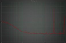
Noise plot is attached, Y scale is in nV/rtHz, X axis in Hz. Noise is higher than the previous version (0.32nV/rtHz) but this can be fed by 2 1.3Ah lead-acid cells. The 60Hz harmonic component is now at 1.5nV equivalent at the input, intermodulation products are still visible.
Can't do better in my allegedly EM polluted environment. Note that a cell phone or drill has absolutely no effect, the thick aluminum block shields perfectly everything that goes over 100Hz.
If so, it would be nice to see the difference if any in noise spectrum when fed from your Agilent PSU.
Hans
Was this spectrum recorded with 1.3Ah lead-acid batteries ?
If so, it would be nice to see the difference if any in noise spectrum when fed from your Agilent PSU.
Yes, from batteries. Nothing unexpected with the 6627A Agilent PS, slightly higher 60Hz (about 2nV) and some 2nd and 3rd 60Hz harmonics creeping from the noise floor (these are almost in the noise floor for batteries). Obviously batteries are better, nobody ever debated that.
The purpose of this experiment was to figure out if it's possible to completely eliminate the spurious mains components, even with batteries and ideal shielding. The answer is no, it is not possible in my lab.
Last edited:
My latest low noise instrumentation amplifier.
- JFET based (8 in parallel, yes Gerhard, is rock solid stable
- 0.3Hz to 1.8MHz 3dB bandwidth
- 60.02dB gain
- 0.42nV/rtHz
- 1/f noise corner frequency is 100-150Hz
- needs +/-12V, takes 16mA/10mA so can use batteries
- Onboard ultra low noise LDO regulators
- encased in an aluminum block, 20mm thick walls, 15mm thick lid, about half a kilo of metal
Noise plot is attached, Y scale is in nV/rtHz, X axis in Hz. Noise is higher than the previous version (0.32nV/rtHz) but this can be fed by 2 1.3Ah lead-acid cells. The 60Hz harmonic component is now at 1.5nV equivalent at the input, intermodulation products are still visible.
Can't do better in my allegedly EM polluted environment. Note that a cell phone or drill has absolutely no effect, the thick aluminum block shields perfectly everything that goes over 100Hz.
Impressive built as always, but
I wouldn't call it an instrumentation amplifier (InAmp).
A question, is it right to compensate the peaking caused by the C seen from the low Z CFA feedback loop (at the inverting input) by adding an input L?
Stein
Last edited:
Impressive built as always, but
I wouldn't call it an instrumentation amplifier (InAmp).
A question, is it right to compensate the peaking caused by the C seen from the low Z CFA feedback loop (at the inverting input) by adding an input L?
Stein
Instrumentation, yes, I should call it "precision", "Instrumentation" is taken by a specific circuit topology.
Theoretically, paralleling JFETs can create a stability problem, in particular for low impedance sources, and that's because from certain frequencies up, the JFET input impedance can get negative. The purpose of the inductor is to avoid such, by increasing the source impedance at high frequencies, without adding to the noise (as a resistor would do). Experimentally, 1uH is enough to stabilize the amplifier for any source impedance, I tried up to 64 BF862 in parallel.
There are many other ways to stabilize a JFET gain stage against this negative input impedance, see http://www.polyfet.com/mtt97.pdf Unfortunately I don't think any other method known from RF amplifiers applies at low frequencies. Adding a gate inductor is essentially not different from adding a ferrite bead on the gate pin, only that this would be more difficult for a SOT23 SMD device
.BTW, this is not single pole compensated, otherwise the 1.8MHz closed loop bandwidth would map to a 1.8GHz GBW, impossible.
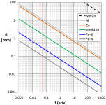
From a consideration of skin-depth a few mm of steel is better than several cm of aluminium for screening, particularly if mains frequencies are the issue.- encased in an aluminum block, 20mm thick walls, 15mm thick lid, about half a kilo of metal
Instrumentation, yes, I should call it "precision", "Instrumentation" is taken by a specific circuit topology.
Theoretically, paralleling JFETs can create a stability problem, in particular for low impedance sources, and that's because from certain frequencies up, the JFET input impedance can get negative. The purpose of the inductor is to avoid such, by increasing the source impedance at high frequencies, without adding to the noise (as a resistor would do). Experimentally, 1uH is enough to stabilize the amplifier for any source impedance, I tried up to 64 BF862 in parallel.
There are many other ways to stabilize a JFET gain stage against this negative input impedance, see http://www.polyfet.com/mtt97.pdf Unfortunately I don't think any other method known from RF amplifiers applies at low frequencies. Adding a gate inductor is essentially not different from adding a ferrite bead on the gate pin, only that this would be more difficult for a SOT23 SMD device
BTW, this is not single pole compensated, otherwise the 1.8MHz closed loop bandwidth would map to a 1.8GHz GBW, impossible.
Good then we agree that it's not an Instrumentation amplifier.
BTW: it seem like you dont understand my question and prefere to answer a question that I have never asked.
I agree with what you put up in your "answer" but that was not my point.
Stein
Good then we agree that it's not an Instrumentation amplifier.
BTW: it seem like you dont understand my question and prefere to answer a question that I have never asked.
I agree with what you put up in your "answer" but that was not my point.
I'm sorry I missed your question; after reading again, I have to admit the question is still escaping me so you may want to further explain and perhaps illustrate.
I'm sorry I missed your question; after reading again, I have to admit the question is still escaping me so you may want to further explain and perhaps illustrate.
My question was:
is it right to compensate the peaking caused by the C seen from the low Z CFA feedback loop (at the inverting input) by adding an input L?
Stein
My question was:
is it right to compensate the peaking caused by the C seen from the low Z CFA feedback loop (at the inverting input) by adding an input L?
Stein
Interesting question, but it belongs in an CFA thread IMHO.
Hans
My question was:
is it right to compensate the peaking caused by the C seen from the low Z CFA feedback loop (at the inverting input) by adding an input L?
My answer is:
I don't know. I did not specifically compensate for the peaking caused by the C seen from the low Z CFA feedback loop (at the inverting input) by adding an input L.
From a consideration of skin-depth a few mm of steel is better than several cm of aluminium for screening, particularly if mains frequencies are the issue.
Set aside the machining issues, I wish it were that easy/simple; regular carbon steel has a permeability of only 100 and OTOH the resistivity of carbon steel is 5x the resistivity of aluminum. Since the skin depth varies with square root of the ratio of these, the improvement in skin depth of steel over aluminum is only 4x. That is, if 2cm of aluminum are required, then the carbon steel equivalent will need 5mm.
Pure iron is so much better, but impossible to source. The ideal magnetic shielding would be a double box of mumetal, but those are expensive hence reserved for professional use. Plus the required annealing, not something one can do at home.
Attachments
Last edited:
Set aside the machining issues, I wish it were that easy/simple; regular carbon steel has a permeability of only 100 and OTOH the resistivity of carbon steel is 5x the resistivity of aluminum. Since the skin depth varies with square root of the ratio of these, the improvement in skin depth of steel over aluminum is only 4x. That is, if 2cm of aluminum are required, then the carbon steel equivalent will need 5mm.
Pure iron is so much better, but impossible to source. The ideal magnetic shielding would be a double box of mumetal, but those are expensive hence reserved for professional use. Plus the required annealing, not something one can do at home.
Ah, yes I think I was assuming generic steel was as good as iron or laminations. Still its better than aluminium or copper for screening at audio, but at RF you also have to think of lossiness which is why its seldom used for that (skin depths are tiny anyway then).
The head amp in post #375 very low frequency noise (0.2Hz-200Hz), now measured with both the head amp and the measurement amp fed from the same lead acid batteries. Overall gain is 86.8dB.
The 60Hz mains frequency component is now 5nV equivalent at the input, a sharp increase from the well shielded measurement amp (1.5nV, see the previous post). That's to be expected, since the head amp is virtually unshielded at these low frequencies. Third harmonic is also clearly visible (it is totally absent in the measurement amp, so this is coming purely from the head amp). Only 50 averages were taken, since it takes about 5 minutes per sweep (due to the time required for the A/D filter to settle, at these low frequencies).
Flat noise (input shorted) is the same 0.26-0.28nV/rtHz as measured before, but now the 1/f noise region is clearly visible. It is very encouraging that the very low frequency noise is almost purely 1/f (slope is about 12dB/decade, compared to the theoretical 10dB/decade), this is a certain plus over low noise JFETs. Also, the noise corner frequency is 2.5-3Hz, again an excellent value, much superior to JFETs (100-150Hz). The left side slight drop is due to reaching the measurement amp LF bandwidth limit (0.3Hz, as mentioned above).
Now, if we could only combine the LF noise performance of bipolars with the low input current noise of JFETs... not going to happen, so it will remain a pick your poison game.
Attachments
Last edited:
You'll be picking up gravitational waves with that setup soon!
A long way to the ~400dB gain parametric amplifier that is LIGO
.I’m really surprised about the rather huge differences in mains radiation between our locations. I have no idea which of the two can be called exceptional, but I think that I must be quite happy getting a flat noise spectrum with an unshielded Head Amp producing just 0.32nV/rtHz.The head amp in post #375 very low frequency noise (0.2Hz-200Hz), now measured with both the head amp and the measurement amp fed from the same lead acid batteries. Overall gain is 86.8dB.
The 60Hz mains frequency component is now 5nV equivalent at the input, a sharp increase from the well shielded measurement amp (1.5nV, see the previous post). That's to be expected, since the head amp is virtually unshielded at these low frequencies. Third harmonic is also clearly visible (it is totally absent in the measurement amp, so this is coming purely from the head amp). Only 50 averages were taken, since it takes about 5 minutes per sweep (due to the time required for the A/D filter to settle, at these low frequencies).
Flat noise (input shorted) is the same 0.26-0.28nV/rtHz as measured before, but now the 1/f noise region is clearly visible. It is very encouraging that the very low frequency noise is almost purely 1/f (slope is about 12dB/decade, compared to the theoretical 10dB/decade), this is a certain plus over low noise JFETs. Also, the noise corner frequency is 2.5-3Hz, again an excellent value, much superior to JFETs (100-150Hz). The left side slight drop is due to reaching the measurement amp LF bandwidth limit (0.3Hz, as mentioned above).
Now, if we could only combine the LF noise performance of bipolars with the low input current noise of JFETs... not going to happen, so it will remain a pick your poison game.
Hans
If these results from 15 years ago are any indication, they may not only be quieter, but are in fact quite likely to. (Still not as quiet as a very good regulator though, by the looks of it.)4 NiMH AA batteries may be better then the lead Acid. 2.2AH 2.8v min and many charge more cycles. They have to be the Precharged low leakage types.
You mean LSD NiMH cells (Low self discharge - they're not that trippy), as pioneered by Sanyo with their Eneloops in the mid-2000s. Makes sense that those with the lowest self-discharging would be the quietest.
This makes me wonder: Can you characterize cells for self-discharge by their 1/f noise, e.g. to weed out any bad apples with internal shorts? Almost seems like it. Hmm. I wonder whether a decent balanced mic preamp will do, 'cause I definitely have some of those...
I must come back to the stability issue of these composite FET amplifiers.
I tried to launch a discussion in usenet sci.electronics design but there were no
takers, so I simply cut & paste it here:
%< ---- %< ---- %< ---- %< ---- %< ---- %< ---- %< ---- %< ----
Let there be an amplifier consisting of one or more CS input JFETs,
an optional cascode, an op amp for plenty loop gain and feedback
into the source. Everybody and his dog does this, but it has
a drawback: it is not stable.
If you measure into the input, you see a capacitance in series with
a resistance. Unfortunately, the resistance may be negative over
a large range of frequencies. That means that with a suitable
inductance at the input, one gets a undamped RLC series circuit,
aka oscillator.
The usual remedy would be a gate/base stopper. Just insert a resistor
into the gate that is more positive than the worst negative value
and you're done. But bandwidth and noise performance are gone.
The next step is that people insert ferrite beads into the gates
and claim victory. But that's Pyrrhus@work or worse.
The beads don't provide a loss resistance at, say, 100 KHz. And
if they did, they would also provide the thermal noise that belongs
to it, so a real resistor is just as good with less guesswork.
Below a MHz, these beads can be inductors with excellent Q, I have
put them on the bridge.
This circuit is fig. 3.34 from Art Of Electronics V3 with a little
different biasing that doesn't matter, I used sth. different as
a starting point.
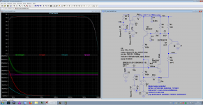
< Bildschirmfoto vom 2020-05-22 04-36-30 | Gerhard Hoffmann | Flickr >
Some observations:
1. I used 16 pcs. CPH3910 in parallel. Sources must be RF grounded
with a distributed array of capacitors or one finds 2V at 500 MHz
there. This is a parasitic loop in the loop, Spice cannot see it
because it cannot see the parasitics. Even 2 nF has no impact on
the global loop dynamics.
2. For the feedback, the FETs are common gate. The gates being
the fb reference, they must have known potential. The 1 Meg
does not provide that at RF. There must be some capacitance
from gate to GND.
3. R25 C11 are from experiments to save as much input impedance
as possible while providing the RF gate-gnd connection.
4 The FET sources are a low impedance input. That may change
the feedback factor / overall gain by loading the fb divider slightly.
5. AOE3 mentions a slight overshoot that is easily tamed. But
really, the circuit is not stable. I have checked this with
a lot of published circuits of this architecture and none of them
was blameless, including mine.
6. V(vin) / I(v4) is the input impedance, as seen from the signal
source. re() is the real part of this, the yellow trace in the
upper plotting pane. The real part turns negative between 100 KHz
and 20 MHz, as indicated by the 180° phase flip. The negative
resistance is up to 500 Ohms. (yellow trace)
7. It does not only happen in simulation but also in real life:
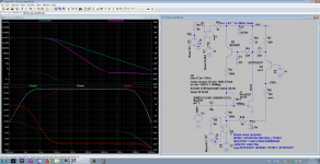
< Bildschirmfoto vom 2020-05-22 04-34-59 | Gerhard Hoffmann | Flickr >
is the behavior of a similar circuit ( with BFT93 folded cascode
and 2 lower gain op amps as an attempt to minimize phase shift).
8. It looks somewhat confusing, but the red line gets outside the
unity circle of the Smith diagram for S11 and that means unstable.
9. In cartesian coordinates, the return loss S11 is actually 1.5 dB
gain, i.e. we get more energy from the input port than we send into it.
(blue)
10. The pink trace is the real part of Zin as computed from S11, and
it is negative over some of the frequency range.
11. I can recommend the DG8SAQ VNWA, you get a lot of capabilities
for a limited amount of money. In fact, it is much less user hostile
than my ZVB8.
%< ---- %< ---- %< ---- %< ---- %< ---- %< ---- %< ---- %< ----
and, as a reply to the only on-topic answer that came from P.Hobbs,
a well known opto-electronics specialist:
I'd like to have only 2 pairs of 18650 lithium batteries, maybe
+-7V when nearly empty ( discharge end is even lower, but I'm
willing to do compromises).
That calls for a folded cascode to use up all available battery
voltage. Therefore, a PNP is needed. Dying species.
Cascode current was 5 to 16 mA, it should be sufficient.
1 MHz BW would be OK.
I had also a normal cascode with 2+4 cells or even more. That
helps the low-noise gain of the FET/BJT with the larger load
resistor.
The cascode does not seem to be the problem, the AOE3 circuit
even works without. OK, the op amp somehow doubles as one.
The circuits behave nicely unless the feedback loop is closed.
When the loop is closed, the source is no longer at GND although
optically it seems so with the half Ohm Rsource.
The source then follows the gate and the FETs could argue that
they do a follower: drain sees the low impedance cascode, source sees
a stiff load, but the voltage at the source lags by the loop delay.
Just like the standard cap-loaded-follower disaster.
At least in simulation it gets much better when i play with VCVS
instead of op amps. But the THS4022 for example brings its own
problems in real life. Local oscillations and huge 1/f noise, for example.
%< ---- %< ---- %< ---- %< ---- %< ---- %< ---- %< ---- %< ----
I could get stable behaviour with _really_ fast opamps
but they would wreck 1/f . And low frequencies is what interests me.
As in choppers, or oscillators close-in to the carrier.
Two pole compensation helps to a degree, the new crop of TI low noise
op amps seems to be better than the AD ones I used, at least in simulation.
Didn't convince in hardware, maybe the dead bug patches go too far
for the existing board.
So I decided to drop the feedback for the input stage. Gone are all
the problems, gain stability vs. temperature is much better than I feared.
It takes a fat PNP with enough emitter current in the folded cascode to
suppress the voltage gain from gate to drain. (Miller killer)
With a BFT93 and low source impedance you can push this to 100 MHz
bandwidth easily. No more op amp influence on 1/f.
The simulation includes 5nV/rtHz of noise on the unfiltered Vcc and Vee,
a requirement that LT3042 or batteries can easily do. The noise contributions
of Vcc and Vee are the red and blue traces in the bottom plot pane, as they
would spoil the input signals.
The ON semi JFET model has no 1/f noise. From the data sheet plots,
the 1/f corner could be down to 30 Hz.
If nobody sees a show stopper, I'll send this to JLCPCB this weekend.
Cheers, Gerhard
I tried to launch a discussion in usenet sci.electronics design but there were no
takers, so I simply cut & paste it here:
%< ---- %< ---- %< ---- %< ---- %< ---- %< ---- %< ---- %< ----
Let there be an amplifier consisting of one or more CS input JFETs,
an optional cascode, an op amp for plenty loop gain and feedback
into the source. Everybody and his dog does this, but it has
a drawback: it is not stable.
If you measure into the input, you see a capacitance in series with
a resistance. Unfortunately, the resistance may be negative over
a large range of frequencies. That means that with a suitable
inductance at the input, one gets a undamped RLC series circuit,
aka oscillator.
The usual remedy would be a gate/base stopper. Just insert a resistor
into the gate that is more positive than the worst negative value
and you're done. But bandwidth and noise performance are gone.
The next step is that people insert ferrite beads into the gates
and claim victory. But that's Pyrrhus@work or worse.
The beads don't provide a loss resistance at, say, 100 KHz. And
if they did, they would also provide the thermal noise that belongs
to it, so a real resistor is just as good with less guesswork.
Below a MHz, these beads can be inductors with excellent Q, I have
put them on the bridge.
This circuit is fig. 3.34 from Art Of Electronics V3 with a little
different biasing that doesn't matter, I used sth. different as
a starting point.
< Bildschirmfoto vom 2020-05-22 04-36-30 | Gerhard Hoffmann | Flickr >
Some observations:
1. I used 16 pcs. CPH3910 in parallel. Sources must be RF grounded
with a distributed array of capacitors or one finds 2V at 500 MHz
there. This is a parasitic loop in the loop, Spice cannot see it
because it cannot see the parasitics. Even 2 nF has no impact on
the global loop dynamics.
2. For the feedback, the FETs are common gate. The gates being
the fb reference, they must have known potential. The 1 Meg
does not provide that at RF. There must be some capacitance
from gate to GND.
3. R25 C11 are from experiments to save as much input impedance
as possible while providing the RF gate-gnd connection.
4 The FET sources are a low impedance input. That may change
the feedback factor / overall gain by loading the fb divider slightly.
5. AOE3 mentions a slight overshoot that is easily tamed. But
really, the circuit is not stable. I have checked this with
a lot of published circuits of this architecture and none of them
was blameless, including mine.
6. V(vin) / I(v4) is the input impedance, as seen from the signal
source. re() is the real part of this, the yellow trace in the
upper plotting pane. The real part turns negative between 100 KHz
and 20 MHz, as indicated by the 180° phase flip. The negative
resistance is up to 500 Ohms. (yellow trace)
7. It does not only happen in simulation but also in real life:
< Bildschirmfoto vom 2020-05-22 04-34-59 | Gerhard Hoffmann | Flickr >
is the behavior of a similar circuit ( with BFT93 folded cascode
and 2 lower gain op amps as an attempt to minimize phase shift).
8. It looks somewhat confusing, but the red line gets outside the
unity circle of the Smith diagram for S11 and that means unstable.
9. In cartesian coordinates, the return loss S11 is actually 1.5 dB
gain, i.e. we get more energy from the input port than we send into it.
(blue)
10. The pink trace is the real part of Zin as computed from S11, and
it is negative over some of the frequency range.
11. I can recommend the DG8SAQ VNWA, you get a lot of capabilities
for a limited amount of money. In fact, it is much less user hostile
than my ZVB8.
%< ---- %< ---- %< ---- %< ---- %< ---- %< ---- %< ---- %< ----
and, as a reply to the only on-topic answer that came from P.Hobbs,
a well known opto-electronics specialist:
I'd like to have only 2 pairs of 18650 lithium batteries, maybe
+-7V when nearly empty ( discharge end is even lower, but I'm
willing to do compromises).
That calls for a folded cascode to use up all available battery
voltage. Therefore, a PNP is needed. Dying species.
Cascode current was 5 to 16 mA, it should be sufficient.
1 MHz BW would be OK.
I had also a normal cascode with 2+4 cells or even more. That
helps the low-noise gain of the FET/BJT with the larger load
resistor.
The cascode does not seem to be the problem, the AOE3 circuit
even works without. OK, the op amp somehow doubles as one.
The circuits behave nicely unless the feedback loop is closed.
When the loop is closed, the source is no longer at GND although
optically it seems so with the half Ohm Rsource.
The source then follows the gate and the FETs could argue that
they do a follower: drain sees the low impedance cascode, source sees
a stiff load, but the voltage at the source lags by the loop delay.
Just like the standard cap-loaded-follower disaster.
At least in simulation it gets much better when i play with VCVS
instead of op amps. But the THS4022 for example brings its own
problems in real life. Local oscillations and huge 1/f noise, for example.
%< ---- %< ---- %< ---- %< ---- %< ---- %< ---- %< ---- %< ----
I could get stable behaviour with _really_ fast opamps
but they would wreck 1/f . And low frequencies is what interests me.
As in choppers, or oscillators close-in to the carrier.
Two pole compensation helps to a degree, the new crop of TI low noise
op amps seems to be better than the AD ones I used, at least in simulation.
Didn't convince in hardware, maybe the dead bug patches go too far
for the existing board.
So I decided to drop the feedback for the input stage. Gone are all
the problems, gain stability vs. temperature is much better than I feared.
It takes a fat PNP with enough emitter current in the folded cascode to
suppress the voltage gain from gate to drain. (Miller killer)
With a BFT93 and low source impedance you can push this to 100 MHz
bandwidth easily. No more op amp influence on 1/f.
The simulation includes 5nV/rtHz of noise on the unfiltered Vcc and Vee,
a requirement that LT3042 or batteries can easily do. The noise contributions
of Vcc and Vee are the red and blue traces in the bottom plot pane, as they
would spoil the input signals.
The ON semi JFET model has no 1/f noise. From the data sheet plots,
the 1/f corner could be down to 30 Hz.
If nobody sees a show stopper, I'll send this to JLCPCB this weekend.
Cheers, Gerhard
Attachments
Last edited:
- Home
- Source & Line
- Analogue Source
- Richard Lee's Ultra low Noise MC Head Amp