One more follow-up ?? for HPS6.2
Thanks Ovidiu,
a couple of (I hope) final comments:
(Although I started down the HPS5.1 path, I never quite finished, so I am still enjoying my 3.1 daily.)
First, I followed a link someone posted to JLCPCB.com as I wondered how they could supply boards so cheaply - They pointed out that your Gerber TOP file had no board outline so they cancelled my order. I guess not being able to center on a 100 square board is how they save money. I dug out my old ORCAD to draw one in and it told me I needed to upgrade to Windows 3.1 to run ORCAD (does that reveal my age?). I'll try Altium at work tomorrow. If that doesn't work, who does your boards?
Second, I am not finding a P channel jfet called PN4362 is that the correct number?
Hi Ken,
I have done a few pcbs with jlcpcb. I got it to load, you need to re-name the files to their naming convention and in the quote system provide the pcb dimensions which are 124x81mm. I figured that out with Gerbtool, 4900x4200 mil, as the board outlines came through with the top and bottom gerber files.
It will auto figure out the board outline if you provide a fab/drill drawing.
Since the pcb is >100mm in any direction, you do not get the special deal, but still I have it quoted at $9.98CDN, plus slow boat shipping, it comes out to just over 20 for 5 of them.
PN4362? where is that being used?
If Ovidiu, was to be so kind as to provide me the design, I could dress it up, generate a BOM with distributor part numbers etc. I would not distribute it in any way without permission.
Attachments
Last edited:
Thanks Ovidiu,
a couple of (I hope) final comments:
(Although I started down the HPS5.1 path, I never quite finished, so I am still enjoying my 3.1 daily.)
First, I followed a link someone posted to JLCPCB.com as I wondered how they could supply boards so cheaply - They pointed out that your Gerber TOP file had no board outline so they cancelled my order. I guess not being able to center on a 100 square board is how they save money. I dug out my old ORCAD to draw one in and it told me I needed to upgrade to Windows 3.1 to run ORCAD (does that reveal my age?). I'll try Altium at work tomorrow. If that doesn't work, who does your boards?
Second, I am not finding a P channel jfet called PN4362 is that the correct number?
https://www.onsemi.com/pub/Collateral/MMBF4391LT1-D.PDF
Did the boards with jlcpcb, got no complaints about the board outline. Attached are the files used to manufacture the boards (downloaded from my jlcpcb account).
Attachments
Last edited:
Hi Ken,
I have done a few pcbs with jlcpcb. I got it to load, you need to re-name the files to their naming convention and in the quote system provide the pcb dimensions which are 124x81mm. I figured that out with Gerbtool, 4900x4200 mil, as the board outlines came through with the top and bottom gerber files.
It will auto figure out the board outline if you provide a fab/drill drawing.
Since the pcb is >100mm in any direction, you do not get the special deal, but still I have it quoted at $9.98CDN, plus slow boat shipping, it comes out to just over 20 for 5 of them.
PN4362? where is that being used?
If Ovidiu, was to be so kind as to provide me the design, I could dress it up, generate a BOM with distributor part numbers etc. I would not distribute it in any way without permission.
Ken is looking at another design posted in this thread, using a JFET cascode.
You mean, the Orcad files?
yes the orcad filesI'll sign your NDA
Let me check if I can still open those 2 years old files for clean up, Orcad got since several versions and updates. Since 2017, Orcad no longer supports the classic Layout. I'm slowly migrating myself to KiCad, already have a project completed (a low noise 60dB instrumentation amplifier).
Don't set your hopes to high, Orcad can generate BOMs, but transforming the output in an usable shopping list is very hard work. I never bothered with, so the files may not be ready for.
Last edited:
I'll try, I know no guarantees
That is too bad orcad layout died, not sure waht version you stopped at. I still have mine running, sort of so I can read in your files if they are complete. I can tell you places where to look, but it depends on where you put them.
You do not need to open them, but I need the referenced libraries, esp the capture ones.
project, *.opj
capture design, *.dsn, *.dbk
netlist for layout, *.mnl
layout, *.max
layout back annotation, *.swp
layout libraries, *.llb
capture library, *,olb
I have lots of orcad libraries that have the properties formatted for easy upload to a distributor, but as you know a good part of doing cad is library work.
I can replace your library parts with mine or merge with mine
thx Rick
That is too bad orcad layout died, not sure waht version you stopped at. I still have mine running, sort of
so I can read in your files if they are complete. I can tell you places where to look, but it depends on where you put them.You do not need to open them, but I need the referenced libraries, esp the capture ones.
project, *.opj
capture design, *.dsn, *.dbk
netlist for layout, *.mnl
layout, *.max
layout back annotation, *.swp
layout libraries, *.llb
capture library, *,olb
I have lots of orcad libraries that have the properties formatted for easy upload to a distributor, but as you know a good part of doing cad is library work.
I can replace your library parts with mine or merge with mine
thx Rick
Hello,
Is there additional data available for the HPS6.1? I am coming from HPS5.1 that was a fantastic sounding amplifier. The downside was a poor phase margin and a huge temperature dissipation. Has the stability been improved in the new implementation?
Remus
Not sure how you concluded HPS5.1 has a phase marging problem, I never seen or heard about such. Perhaps you mean the low frequency fluctuations? Those are not instabilities, but unavoidable (in a single ended approach) fluctuations of thermal origin.
It's running pretty hot, yes, and so does HPS6.1 (the mai difference is the new servo, greatly increasing the PSRR, therefore greatly simplifying the power supply, and the use of the new low noise regulators from TI - there's a version with standard regulators, no performance difference).
If heat is an issue, get HPS6.2, that could be even fed from batteries (withing certain constraints, no switchable gain and slightly higher noise at 0.5nV/rtHz).
Not sure how you concluded HPS5.1 has a phase marging problem, I never seen or heard about such. Perhaps you mean the low frequency fluctuations? Those are not instabilities, but unavoidable (in a single ended approach) fluctuations of thermal origin.
Hello,
you are correct, i do mean the low frequency fluctuations, im sorry for creating a confusion. Are these eliminated now?
Regarding the heat, do you think that mounting the bottom of the PCB close to the chassis with a thermal transfer compound would pose a problem?
What is the current consumption of the HPS6.1? Would i be able to use the power supply used for HPS5.1? I have 750mA per secondary available and about 32V on the filtering caps, can the on-board regulators handle the voltage drop across them as well as power dissipation?
Thanks
Not completely, they are unavoidable in single ended high gain (around 86dB at LF) amplifiers. These fluctuations are of thermal origin and would be largely avoided by lowering the input stage current (hence the power dissipation), like in HPS 6.2 (comes with some noise penalty, though).
Any cooling method is acceptable and would help with the fluctuations, assuming you isolate the board from the chassis.
HPS 6.1 takes some 140mA worst case, with the gain relay activated, otherwise about 120mA, this is from the positive power supply, per channel. The negative power supply current is very low. The 5.1 power supply is more than enough for HPS 6.1. Make sure you minimize the voltage drop across the LDO voltage regulators, they don't need more than 0.5V to be in spec and you don't want them to run uselessly hot. Either adjust the output voltage, or use bleeder resistors on the unregulated power inputs.
Once again, if you are not sure you can solder the LDO DFN packages (it is not trivial, requires hot air soldering tools and good skills) use the version with LM317/LM337 regulators (Gerbers and schematics in the same thread), without any performance penalty, those will also be much more tolerant to power dissipation.
Last edited:
Hi Ovidiu.
Am I missing something? I checked your schematics and:
1. Both in HPS6.1 and in 6.2 the feedback resistor dividers for TPS7A4701 and TPS7A33 seem to be designed for a very low output voltage. You would get +-18V only if R504 would be 20k instead of 200k and R501 16.5k instead of 165k. Am I right?
2. Looking at HPS6.1 it seems the bipolars in the cascodes are not properly polarized (Q209 to Q216): 1N4735 drives the base voltage to ~6.2V, while the collector voltage is ~25% of VCCL (4.5V based on R222 of 1Meg and R228 of 330k). The bipolars are saturated and can't work. Maybe some component values are not right?
Last edited:
Hi Ovidiu.
Am I missing something? I checked your schematics and:
1. Both in HPS6.1 and in 6.2 the feedback resistor dividers for TPS7A4701 and TPS7A33 seem to be designed for a very low output voltage. You would get +-18V only if R504 would be 20k instead of 200k and R501 16.5k instead of 165k. Am I right?
2. Looking at HPS6.1 it seems the bipolars in the cascodes are not properly polarized (Q209 to Q216): 1N4735 drives the base voltage to ~6.2V, while the collector voltage is ~25% of VCCL (4.5V based on R222 of 1Meg and R228 of 330k). The bipolars are saturated and can't work. Maybe some component values are not right?
1. Values are wrong, R402=R403=R502=R503=240k, R404=R504=20k, R401=R501=16.5k See below the comment about the board photo.
2. You are again correct, values on the schematic are wrong. R222=R322=2Meg R228=R328=1Meg so the voltage should be ~6V.
The Zener diodes D201, D301 are any 3.3V in SOD-323 case.
I apologize for these issues, the root cause is that in Orcad it is impossible (or very difficult) to use the same schematic for simulation and board layout. Once you decide for the topology, you assign the devices footprints and start routing the board; in parallel you can calculate and then run simulations to optimize the device values. This makes the schematics to diverge. I should have updated the board schematics in #1 with the right values.
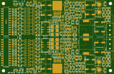
As a rule, when something looks wrong, check the board photo (that's why I posted large board photos in #1 and the following). I can guarantee those values are correct, since those are fully working boards.
P.S. I see I can edit #1, I will try to update the schematic archive as soon as I have the time to make the corrections and double check them.
Last edited:
Thanks for the update of the HPS 6.1 component values!
Which is the current set point for the input stage in case I plan to run HPS 6.2 at +-18V?
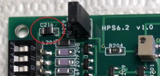
C216 & C316 from HPS 6.2 are indeed 1u / 50V film type? From the picture they look like Panasonic ECP-U1C105MA5. Any film @50V would be quite large for the footprint.
Which is the current set point for the input stage in case I plan to run HPS 6.2 at +-18V?
C216 & C316 from HPS 6.2 are indeed 1u / 50V film type? From the picture they look like Panasonic ECP-U1C105MA5. Any film @50V would be quite large for the footprint.
Thanks for the update of the HPS 6.1 component values!
Which is the current set point for the input stage in case I plan to run HPS 6.2 at +-18V?
C216 & C316 from HPS 6.2 are indeed 1u / 50V film type? From the picture they look like Panasonic ECP-U1C105MA5. Any film @50V would be quite large for the footprint.
Please check again, C216 & C316 are ceramic 0.1uF decoupling on the schematic. The two 1uF caps are both ceramic, X7R, 1206
Please check again, C216 & C316 are ceramic 0.1uF decoupling on the schematic. The two 1uF caps are both ceramic, X7R, 1206
I mean the one in the picture. This is film type or am I wrong? A ceramic in this place is strongly not recommended.
Attachments
I mean the one in the picture. This is film type or am I wrong? A ceramic in this place is strongly not recommended.
Sorry I was looking at HPS 6.1. Yes, the cap is film 1206 in size DigiKey 338-4076-1-ND or equivalent. Any value between 0.1u and 1u is good enough in that position.
JFETs are running at about 1mA each, total 8mA.
Last edited:
Not sure why the forum software is not letting me to edit the attachments, nevertheless find attached the updated schematics for HPS6.1. Keep checking against the board photo in #1 when in doubt.
One last (hopefully) correction: Zener diodes for the cascode are 3.3V in SOD323, for example DigiKey MM3Z3V3BCT-ND or equivalent.
One last (hopefully) correction: Zener diodes for the cascode are 3.3V in SOD323, for example DigiKey MM3Z3V3BCT-ND or equivalent.
Attachments
Last edited:
- Status
- This old topic is closed. If you want to reopen this topic, contact a moderator using the "Report Post" button.
- Home
- Source & Line
- Analogue Source
- HPS 6.1