The AD797 is an under-compensated opamp, sometimes requiring a capacitor to pin 8.
Reading the very comprehensive data sheet, it is an awkward device for supply decoupling and capacitive load driving. Your single sided pcb does not look suitable for a fast part like this.
Sorry to take so long to reply but been doing lots of etching / recovering from etching then soldering & finally back to testing my RIAA circuit & found the AD979 does not work in my circuit now anyway, so went back to the opa134 instead.
Is there a super chip op-amp I could use instead of the ad797 or is there little difference is sound to be had ?
I see several problems here:
A) Your RIAA filter values are not the same as the two JLH RIAA schematics I found. R6 has different value and there's a missing link between components.
B) You can't just add over 100K to the feedback network and expect it to still conform to RIAA curve, it won't. It needs to be 5K6.
C) without any additional DC blocking C's you're likely to get a large DC offset at output of 2nd opamp which will limit headroom.
As you have it, the bass will be 10dB too low and the treble 10dB too high, also some deviations in the midrange.
I would put all the 1st stage feedback network component back to the JLH values and then change/reduce the gain of the second stage as needed.
See JLH Hart preamp 2/3rds down this page:
A Paul Kemble web page - John Linsley Hood preamp designs.
and the opamp version here:
John Linsley Hood K1500 Shunt Feedback MM and MC RIAA Pickup Preamp
Thank you for your help & just re-read what you said about a missing link & tonight I just realised where I had gone wrong on my prototype & added the link, now the prototype is working perfect as this circuit had no treble but did not want to say anything on here until I had found the fault & fixed it as I could not understand why the treble was missing on every single type of op-amp I used ! (I was not understanding at the time what you meant, lol (darn ferric chloride on the brain))
I would also like to say thanks for the re-worked riaa pre amp circuit you have provided me to make which I will do once I have tested yet another prototype I had already etched but not yet soldered components to.
If this next one is not successful your design will be next on the list for design / etching etc.
Thanks all for you input
J247W
I have great results with AD847, LM4567 and OPA627.
Thanks, I am running the OPA134's in by leaving it powered, just tried it & the bass has improved & the treble is cleaner may leave it for a week or 2 powered to run those op-amps in.
Will get hold of those op-amps 2 at a time to test on my prototype, so I have a standard circuit for testing different op-amps.
Does the battery power option remove any noise or lower the signal to noise ratio much ?
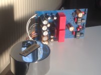
Battery supply is the most quiet design i have build. It is also easy to build. Just 2 x 9v batteries and solar charger. About 12 hours of continue play.
lm4562 MM phonostage on solar energy.
lm4562 MM phonostage on solar energy.
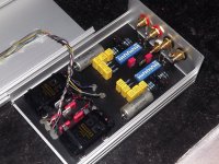
Very interesting question. Ground plane PCB's provides lowest level of hum and avoid unwanted RF reception (mostly used only for RF devices). That is a great benefit if there is required a high gain.Before I begin to etch my latest RIAA Pre-Amp design I just wanted some experienced peoples design knowledge on RIAA layout design.
I know that to avoid hum & microphonic noise I have to be carful around the RIAA filters but what about the rest of the circuit, I am used to etching pre amp designs fully screened but record player pre design seems a lot more sensitive maybe it's something I have not thought of.
I would like to discuss the design in detail to make sure I don't etch a fail design costing pennies per board ?
Thanks
J247W
OTOH - very important it is to know, that there are rises up parasitic capacitors at several places.
Any nodes, where capacitances to GND are critical and unwanted should be elevated from copper ground plane so that they are as far away from the copper surface as possible.
I don't understand the marked term. Mean you this only for the showed circuit or in general ?Certainly AD797 is a total waste - there'll be too much noise from all those high value R's, particularly R3. The feedback network doesn't look right for RIAA. R7,8,9 are redundant.
Your copper pour areas are not doing anything as they are all floating, normally they'd be connected to GND.
If I etch a board I don't usually bother with ground plane / copper pour, I always use a metal case which does a much better screening job.
If I machine a board with CNC router, then I use copper pour to save machine time and don't worry about small floating copper islands.
A special feature of the AD797 is the fact, that there is only one voltage gain stage in the NFB loop (like OPA604, OPA2604, OPA2134 and any few other).
Most other uses two voltage gain stages like NE5532 or NE5534.
Check out
AD797 discrete clone - comparison of seven variations
and the URL's mentioned there.
Last edited:
Only for the showed circuit, definitely not in general.I don't understand the marked term. Mean you this only for the showed circuit or in general ?
- Status
- This old topic is closed. If you want to reopen this topic, contact a moderator using the "Report Post" button.
- Home
- Source & Line
- Analogue Source
- RIAA - Copper fill or no copper fill?