Great!
Also, I think I would have drawn the MC stage a little different. I would move R22/R38/R55/R37 and C44/C24/C52/C39, from the PSU schematic to the MC schematic.
The MC stage is similar to the one QUAD used and is typically drawn with these components together with the rest of the curcuit.
The capacitor and resistor from base to emitter pusle me a bit. The resistors might be an option for trimming the difference in base current of the two transistors.
Mogens
yes, the place of the resistors R45/79 and R78/83 is unused - the SMD-caps are very small values, so I think (to prevent oscillation), unfortunately SMD chip caps without marking code in most cases.
Back to the output stage. According the previous URL resp. second image in this post the schematic from previous post is still wrong and should actually look like in the first image of this post. But according the PCB of "micro iphono 2", ser.-No 2042002252 the schematic looks definitely like the correction in my previous post.
Such a version I don't find online anywhere - have a look to the other schematics in the additional attachments.
Either it really is a design flaw that has crept in between the prototype and mass production stages (the fact, that the device works, does not mean automatically, that everything was done right) or it's a special version for a special sound character.
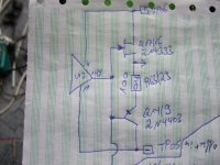
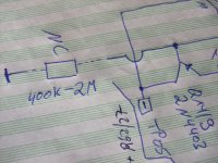
The measured resistance between Gate/Base of the output stage and GND is 400 K in one polarity and 2000 K (2 M) in the other polarity.
That means, that no external resistor was overlooked and the measured values are defined by the internal circuit structure of U2.
Maybe one of the members know more about it - thank you very much.
This URLs don't provide the right advices:
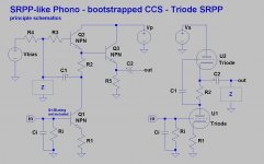
The Good Old Days & More SRPP
Fertige Phono-Vorstufen mit SRPP-Schaltung von Alex Nikitin (wie Creek OBH-8) - Phonovorstufen und Ubertrager - Analogue Audio Association
Attachments
Last edited:
No, I don't think your original drawing with the resistor R63/29 is in the base of Q14/9 only is necessarily wrong. As I previously said, as I don't have the board myself I can't determine which side of the resistor the gate is tied to. But, it's fine if it's just in the base of Q14/9. The resistor doesn't need to be between source and emitter, like the circuit used in the cross-over. That's just if you want a larger Gate-source voltage in order to reduce the current of the JFet further than the VBE of 0.6V from the PNP transistor alone.
So I think you circuit from post #18 is correct.
Cheers,
Mogens
So I think you circuit from post #18 is correct.
Cheers,
Mogens
The schematic by post 11 under
https://www.diyaudio.com/forums/ana...preamplifier-2006-edition-11.html#post5548073
is very close to the version here (except MC head amp, offset servo and output buffer stage).
https://www.diyaudio.com/forums/ana...preamplifier-2006-edition-11.html#post5548073
is very close to the version here (except MC head amp, offset servo and output buffer stage).
under
Mono and Stereo High-End Audio Magazine: Interview with Thorsten Loesch of iFi - AMR about iFi iPhono
there are some circuit descriptions, but not everything corresponds to the drawn circuit from me.
What means the term "CR-EQ" ??? - go to
RIAA CR型イコライザー回路の計算
Maybe without inductors (with Inductors = LCR-EQ), maybe RIAA network in the feedback pad and not a passive network between two line stages.
Post #11 was wrong. page 11 and post #101 is correct.The schematic by post 11 under
https://www.diyaudio.com/forums/ana...preamplifier-2006-edition-11.html#post5548073
is very close to the version here (except MC head amp, offset servo and output buffer stage).
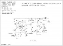
Shortcomings iFi iPhono2 (©2015-V1.3)
There are a lot of shortcomings on iFi's model iPhono2 (©2015-V1.3), from which I have create the schematic.
A) Printing error concerning the device inscription at SW3 for RIAA EQ Graph on bottom of this device
1) eRIAA (DIP 4/5) means in real life IEC (International Electrotechnical Commission) - user selectable IEC-RIAA option, i. e. additional 6db subsonic- resp. rumble filter. eRIAA "On" means actually subsonic "off", because the "ON" position create a bypass across C17/37/40 for the right channel and across C54/53/18 for the left channel. The correct labeling there should actually be "Subsonic on" in the "off" position of DIP4/5 and not "eRIAA".
2) what here IEC means in real live (DIP3/6) I don't know (maybe "eRIAA ? - go to
File:ERIAA.svg - Wikipedia).
In this case one could simply say that the terms "eRIAA" and "IEC" have been reversed, but I don't think, this is right.
DIP3/6 controls the CMOS IC's U4/U5 (4066). In the "ON" position PIN8 and 9 of U4/U5 and thus R74/53 in the RIAA network is shorted.
I doubt if the ordinary RIAA function works in the right matter, because I miss a resistor between the output stage (emitter Q14/9) and the input of the RIAA network, that is in the NFB path (C68/46, R69/87). Therefore, the eRIAA function is also doubtful.
B) Shortcomings affecting reliability and lifetime
1) To ensure a constant current consumption and a higher power consumption than with the iphono2 circuit itself (for additional 100mA), an additional resistor of 150 ohms was introduced between the inputs of the positive and negative rail.
This have folllow consequences:
- With the included, slightly too weak in-wall power supply from AMR Audio model "LN-1530" sometimes rises up an undesirable 50Hz hum (by use of an enhanced power supply, where are better parts in use, this issue disappears).
- Despite the fact that 3 pieces 51 ohm resistors were connected in serial mode to distribute the thermal load, some parts become seriously hot, particularly the electrolytic capacitor C4 and the others arround it.
C) Shortcomings affecting sonic quality
1) internal SMPS technology to create internal a neg. rail vs. GND - go to
https://www.onsemi.com/pub/Collateral/MAX828-D.PDF
This means one SPS supply in the pos. rail and two SPS supplies in the neg. rail. Not a really good approach - at least from my view. But a very cost effective solution, because the in wall power supply is an already exist part in a great amount for various other applications.
2) CMOS switches; for the EQ modes "Columbia", "DECCA" and "eRIAA" (what ever it is in real live) there are CMOS switches (4066) in use. A very great benefit at first look is here the fact, that the PCB wires to the actually switch are very short. OTOH - there is an important disadvantage: - see also the paper under
http://www.ti.com/lit/an/slyt612/slyt612.pdf
For example, the resistance of a CMOS switch in the closed position, referred to as the on-resistance or R-on, changes depending on the input voltage. This behavior is usually undesirable and can significantly distort the signal in some applications. This disadvantage prevails the advantage of short leads between the parts - so I think.
3) low quality capacitors both for voltage regulator and RIAA network
except the elcaps from ELNA, series 1644 (for C13/23) there are only no-name, low-cost smd elcaps arround the Non NFB voltage regulator in use - unfortunately with only 16VDC and 6V3DC. Consequence is bad sound already after a short period of use. In general - 50VDC until 63 VDC provides the lowest ESR at 50Hz and 10KHz according the datasheets and thus in this application with low voltage operation very long live time.
Even with the SMD RIAA caps one get the benefit of short wires and small space requirements, but also here prevails the disadvantage: Unwanted microphonic effect. Even in SMD versions are top quality caps available - go to
https://www.ibselectronics.com/pdf/wima_smd_capacitors.pdf
Unfortunately no small design is to realize by use of top quality parts.
OTOH there is no need to design such a RIAA preamp part as extremely small than this model.
4) Mute control unit: There are a jFET with drain at the output and source at GND. Most designers assume, that there are no disadvantages if there are only switches from Signal part to GND, but no switches in serial to the signal path. That's just right for mechanical versions. Unfortunately not with CMOS and like here jFET's.
The next step is the development of possibilities for improvement.
Last edited:
There are a lot of shortcomings ... 2) CMOS switches; for the EQ modes...there are CMOS switches (4066) in use. ... - there is an important disadvantage: - see also the paper under http://www.ti.com/lit/an/slyt612/slyt612.pdf For example, the resistance of a CMOS switch in the closed position, referred to as the on-resistance or R-on, changes depending on the input voltage. .........
The RIAA etc switches terminate in a Virtual Earth. The voltage swing is nearly zero (here, far under 1mV). The THD is nearly zero. Such connections were widely used, with larger signals, in professional mixing consoles for signal routing.
Homebrew outdoor PS with Choke Inductor for iFi's iPhono2
Description of an easy 50/60 Hz diy outdoor power supply with choke coil was puplished in the German magazine from Mr. Holger Barske. Unfortunately the internal issues in the actually RIAA device remain.
Description of an easy 50/60 Hz diy outdoor power supply with choke coil was puplished in the German magazine from Mr. Holger Barske. Unfortunately the internal issues in the actually RIAA device remain.
Attachments
Review and LabReport in HiFi News
three pages include RIAA Error (RIAA Response) and UserGuide PDF
three pages include RIAA Error (RIAA Response) and UserGuide PDF
Attachments
Last edited:
Where is the difference between "eRIAA" and "RIAA" - I see only the difference between shorted (black line) and not shorted subsonic filter capacitors (blue line) ? - go to the second image under "LAB REPORT". There should actually be a difference at the raised area above 18 KHz.three pages include RIAA Error (RIAA Response) and UserGuide PDF
Strange is also the raised area below 100 Hz without subsonic capacitors at the outpout (bass boost). What is therefore the reason (in the schematic there is no such function to discover)?
Additional questions rises up:
1) what benefit is provided upon the use of R81 (4K7, for schematic go to second image post #12, connection betwen the L+R outputs in front of the 100R resistors R62+R27) ?
2) why subsonic function by C53/37, C18/17 and C54/40 in parallel mode located at the output instead at the input and why only 6db ?
3) where is the patented and
so called TubeState ClassA Tri-Brid Amplification circuit ? Maybe the corrected sketch on first attached image under post #18/21 ?
4) by selecting MC mode (MC = ●) the MM stage operates in the inverted mode (MM = -). Whithout consequences for the RIAA-EQ network ?
Unfortunately there are no answers under
Mono and Stereo High-End Audio Magazine: Interview with Thorsten Loesch of iFi - AMR about iFi iPhono
Thank you for advices.
Last edited:
no replies ?
the article under
Cut and Thrust: RIAA LP Equalization | Stereophile.com
gives an idea of why so many different RIAA networks exist in commercial phono RIAA preamp devices
the article under
Cut and Thrust: RIAA LP Equalization | Stereophile.com
gives an idea of why so many different RIAA networks exist in commercial phono RIAA preamp devices
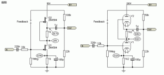
Help with broken iPhono2
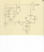
I purchased a used iPhono2 that I would like to fix. The most apparent issue is almost 14V on one of the output channels. The main circuit deviation I've found is the negative supply generation circuit is outputting -7.6V instead of something close to -15V.
I believe I have fully reproduced the negative rail circuit (attached). I have tried replacing both the buck converter (RT6200) and the op-amp, but no change. I have removed an inductor and isolated the circuit from the rest of the board with no change, so it doesn't appear to be a loading issue.
My questions are:
Could the very un-symmetrical supply be the cause of the +14V on one output channel?
Any suggestions on what might be happening with the negative rail circuit?
tiefbassuebertr (who started this thread) did a good job capturing the rest of the circuitry.
Attachments
Thank you for posting this schematic. In the meantime, I also had various devices of this model with similar errors, but I have never done a repair in this sps section just to preserve the genuine condition - check out in this case post #26, C) 1)
Instead, I did the following:
1) All parts removed up to the input of positive and negative rail (TP01/TP02, sixth image post #12)
2) Add of zener diodes between the input of positive and negative rail and GND (ZPY10-ZPY15)
3) Add of an current source with LM317
check out therefore the PS schematic of NAD's phono preamp model "PP2" - go to second PDF in post #5 under
Head Pre for Denon DL 103
4) use not the genuine in wall power supply, but a version with 34VDC-38VDC similar to those under
Original Netzteil SNG-D / FW 3289/H – 10,5V / 34V / 49V – Adapter, Power Supply | eBay
Even in cases where there were no faults, I have done this several times to get a better sound.
In all cases you will get in all respects a better sonic quality, particularly, if one add additional capacitors in parallel to the zeners.
Last edited:
I believe I solved the low negative rail voltage by replacing R15 with a 4.22k resistor. According to the RT6200 this value should provide 15V output with R14 set at 75k. I did this and now have -15V. So I'm not sure if the 10k was a manufacturing error or what.
The voltage appearing on one of the output channels seems to be due to the audio op-amp IC. I ordered a replacement and will report when it is test.
The voltage appearing on one of the output channels seems to be due to the audio op-amp IC. I ordered a replacement and will report when it is test.
rnuss,
Did you managed to fix you item?
I was considering buying used one (working).
But then I find lot of information on frequent failures. So I'm wondering if this happens how hard will be to fix it by myself. I failure can be fixed in power supply module (negative) on board then it's more or less fine for me. But if this actually breaks rest of the board then I don't want to match transistors by myself (at least for the price I will potentially pay for an item which will be 2/3 of new item).
Yes, I did fix this. I think the main issue with this unit is ESD susceptibility. I added a TVS diode between the chassis-ground and the signal ground, and I have not had an issue since.
I had to replace a transistor that is used as a pass transistor for a voltage regulator circuit, that is part of the negative supply rail. This fixed things until I touched the case and zapped it with a static discharge. So I had to replace that transistor again. That's when I added the TVS.
I power my iPhono2 with a linear 15V power supply and prefer it to the wall-wart. In addition I changed out the OPA1654 with an OPA1644 (quad Op-Amp IC) which lowered the noise and made the sound even better.
Overall I believe the sound punches way above its price-point. From what I can tell the early quality issues were addressed at some point. But if you get an early version, like mine, there may be susceptibility issues.
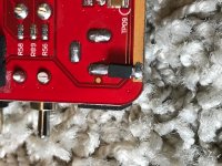
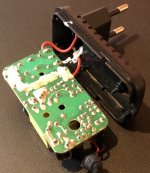
I used a unidirectional TVS (SMAJ30A). There are clear traces on the outside of the pcb that make contact with the case. I just soldered the TVS between that and the ground input from the power supply -see pic. I believe the two grounds are connected with an inductor; I measure ~100 ohms between them.
Attachments
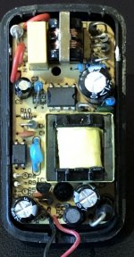
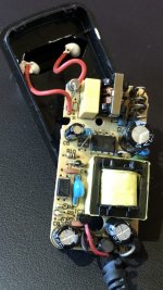
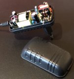
in then attachement the included SMPS (switch mode power supply) in a wall envelope. Schematic and data sheet of the used control-IC is here
http://www.sdc-semi.com/e/UploadFile/SDC608_EN.pdf
not good reliability - mainly through the cheap electrolytic caps and thermal stress - and no screws for disassembly (post #28 shows a better solution).
http://www.sdc-semi.com/e/UploadFile/SDC608_EN.pdf
not good reliability - mainly through the cheap electrolytic caps and thermal stress - and no screws for disassembly (post #28 shows a better solution).
Attachments
-
 40B7FB26-9D77-41EE-9B76-A7773C7F522F.jpeg421 KB · Views: 127
 -
 29333A9A-4BEC-43F8-96AD-7BE2E9131018.jpeg285 KB · Views: 99
 -
 B1FB975C-BE6E-4494-8018-9A08CA6E0AC7.jpeg340.3 KB · Views: 149
 -
 975BFCB5-5BDE-4ED3-B454-C64347F5B471.jpeg415.5 KB · Views: 156
 -
 F99AFA75-0C78-4259-84C0-6FB772CA295E.jpeg397.7 KB · Views: 167
 -
 93B18FCB-EB62-4066-8DB9-52CB9C7D6238.jpeg170.3 KB · Views: 96
Last edited:
I used a unidirectional TVS (SMAJ30A).
Thanks rnuss. I'll probably get my iphono Today.
So if this is unidirectional so what direction have you used (on screenshot I don't see any markings on this part.)?
- Status
- This old topic is closed. If you want to reopen this topic, contact a moderator using the "Report Post" button.
- Home
- Source & Line
- Analogue Source
- iFi Audio Model "micro iPhono2": Creating Schematic - help needed