Hello,
I have been trying to learn how to troubleshoot and repair electronic components by myself (and youtube) and I have decided to go for this little MC/MM preamp, just because there is no schematic online, thinking that it would make things a little more challenging, but I think I have placed myself in a bad position.
After receiving this preamp, I have noticed that the +15V was missing on the OPA2134 but the -15V was clean. Thinking that it may be the 7815, I have replaced it. This let the magic smoke escape in one of the transistors which was right after the AC input. Since the transistor is damaged so badly that I can not read the code anymore, with my utterly limited knowledge I can not figure out what it is. The only remaining text on the front face is "BJ 048" on the bottom line and the top line ends with maybe a "0" followed by "9MA". Can anybody help me solve this mystery? It was a TO-92 package.
Best Wishes,
Dirk
Unknowns ")
You need to determine if it is NPN or PNP and that would be done by measuring the voltages on the empty pads (no transistor fitted) and deducing which is the 'input' (perhaps full unregulated voltage) and which is an 'output' (perhaps low or no voltage) and which is the base (perhaps some indeterminate voltage). TO92 packages also tend to follow a similar lead out pattern.
Another good clue might be to see if there is a mirror image of the transistor used on the negative rail. If so then the zapped one would possibly be its NPN or PNP complement.
The fact its faulty in the first place could be down to a shorted rectifier or shorted or leaky reservoir cap.
Maybe some good pictures would help (no guarantees but you never know)
Pictures! Yes ...
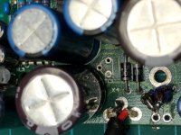
Let me explain what I have attached. This is a dual sided board, the top layer has no connections to the transistor terminals. At the back, there is a 3 pin connection coming from the AC power supply. The two pins on the left share the same pole. These are the ones that get connected to the two terminals of the blown-up transistor. The remaining terminal of the transistor ends up in the NE555 circuit. I think this is a part of the high voltage circuitry to run the 12AX7s.
Please let me know if more pictures are needed.
/Dirk
P.S: I have noticed that the web page rotated the pictures 90 degrees counterclockwise direction.
Attachments
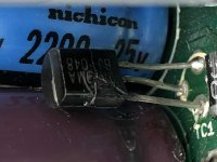
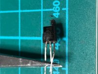

It's not a transistor. It is a 1A triac. Z0109
Z0109NA,412 WeEn Semiconductors | Mouser Belgique
Z0109NA,412 WeEn Semiconductors | Mouser Belgique
Last edited:
Thanks for the pictures.
So a triac. That changes things somewhat
It looks like the gate (middle pin) goes off somewhere (your 555 circuit ?). This is all guesswork without a circuit but I would try and see where that cable goes. The soldering looks a bit scratty (technical term). Is there a short between the red wire and the braid ? Are those two diodes OK ?
Triacs are pretty tough and so whatever happened looks like a catastrophic overload somewhere.
I also can't see any connection between the missing 15 volt rail and the triac... unless there was a short on the rail and that is why it was missing.
This is one that definitely needs a full circuit diagram to figure out.
So a triac. That changes things somewhat
It looks like the gate (middle pin) goes off somewhere (your 555 circuit ?). This is all guesswork without a circuit but I would try and see where that cable goes. The soldering looks a bit scratty (technical term
). Is there a short between the red wire and the braid ? Are those two diodes OK ?Triacs are pretty tough and so whatever happened looks like a catastrophic overload somewhere.
I also can't see any connection between the missing 15 volt rail and the triac... unless there was a short on the rail and that is why it was missing.
This is one that definitely needs a full circuit diagram to figure out.
- Status
- This old topic is closed. If you want to reopen this topic, contact a moderator using the "Report Post" button.