It was 14mV at 0dB gain not 40 mV, giving 1 V at the output, slightly below the 1.4V max.With the 40mV sine wave input signal into the amp, for the working and faulty channel?
OK, just DC voltages first. 9V supply. The regulator is 5V. No signal inputs.
Based on the schematics these three IC are dual channel op amps then.
I will do the measurements with signal input later today.
Vcc, pin 8, voltage is the same for all.
U3 output 1, pin 1, looks like a dead short to the the supply voltage and is different to the other two.
U3 inverting output, pin 2, is low compared to the other two.
Everything looks the same.
Pin 1 = 3.13
Pin 2 = 3.23
Pin 3 = 3.10
Pin 4 = 0.75
Pin 5 = 3.05
Pin 6 = 3.08
Pin 7 = 3.08
Pin 8 = 5.49
U3
Pin 1 = 5.53
Pin 2 = 0.96
Pin 3 = 3.13
Pin 4 = 0.75
Pin 5 = 3.10
Pin 6 = 3.13
Pin 7 = 3.13
Pin 8 = 5.56
U4
Pin 1 = 3.27
Pin 2 = 3.23
Pin 3 = 3.22
Pin 4 = 0.75
Pin 5 = 3.21
Pin 6 = 3.25
Pin 7 = 3.69
Pin 8 = 5.68
Last edited:
Could it be a 49721 or a TL972ID ?
ART DJ Pre II op amps ? | Audiokarma Home Audio Stereo Discussion Forums
http://www.ti.com/lit/ds/symlink/lme49721.pdf
TL972ID pdf, TL972ID description, TL972ID datasheets, TL972ID view ::: ALLDATASHEET :::
Looking at the picture .. the lower op-amp could be a rail-splitter as it is near the supply and You have a single supply jack.
Instead of a signal generator, why don't you just connect a turntable and measure ?
Firstly, I’d like to thank everyone contributing. It is not fun being the weakest link!
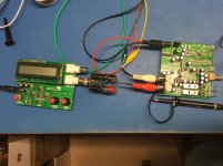
Just so you know how I am testing I have attached a picture. The noise is too much at anything less than 30mV signal. I have shortened all the wiring in an attempt to improve it. Out of shot is a Siglent DSO.
The DC voltages were posted this morning.
Tonight I applied the AC signal to each channel and measured AC signal on U2 and U3. All I saw on U4 was low voltage 50Hz ripple or nothing so I didn’t record the details.
Here is the AC data with the scope AC coupled. Approx 30mV 1000Hz sine wave. Pre-amp gain set to zero.
U2
Input to-> LC RC
Pin 1 = 230mV 1kHz 30mV 50HZ
Pin 2 = 30mV 1 kHz Noise
Pin 3 = 30mV 1kHz Noise
Pin 4 = Noise Noise
Pin 5 = 200mV 1kHz Noise
Pin 6 = 200mV 1kHz but clipped Noise
Pin 7 = 200mV 1kHz 30mV 50Hz
Pin 8 = Noise Noise
U3
Input to -> LC RC
Pin 1 = Noise Noise
Pin 2 = Noise Noise
Pin 3 = 30mV 1kHz Noise
Pin 4 = Noise Noise
Pin 5 = Noise Noise
Pin 6 = Noise Noise
Pin 7 = Noise Noise
Pin 8 = Noise Noise.
Attachments
Thanks for the input. I think I read that post a while ago. Should one of mine need replacing I still,wouldn’t know what would be suitable!
I don’t think it feasible to use a turntable as a source unless I had a tone signal LP - I could be wrong!
I don’t think it feasible to use a turntable as a source unless I had a tone signal LP - I could be wrong!
Could it be a 49721 or a TL972ID ?
ART DJ Pre II op amps ? | Audiokarma Home Audio Stereo Discussion Forums
http://www.ti.com/lit/ds/symlink/lme49721.pdf
TL972ID pdf, TL972ID description, TL972ID datasheets, TL972ID view ::: ALLDATASHEET :::
Looking at the picture .. the lower op-amp could be a rail-splitter as it is near the supply and You have a single supply jack.
Instead of a signal generator, why don't you just connect a turntable and measure ?
Last edited:
So...
That odd reading on pin 1 would seem to indicate an issue.
Your readings seem to indicate U2 is for one channel and U3 for the other, and that the input first goes to the non inverting input of one of the opamps within each package for those IC's.
That is the 30mv on U2 and U3 pin 3
U2 looks to be OK... all reasonable.
U3 DC conditions (if the above theory is correct) look very wrong.
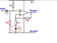
Pin 3 at 3 volts and pin 2 at a significantly lower voltage would drive the opamp output hard to the positive rail. The question is whether the problem is the opamp or the surrounding feedback network.
Can you see whether Pin 2 has a capacitor (probably connected via a series resistor) to ground. If so, is the cap leaky ?
Also can you visually compare components between U2 and U3 to try and confirm the theory that U2 and U3 are handing left and right channels. If so then the circuitry should match between them.
That odd reading on pin 1 would seem to indicate an issue.
Your readings seem to indicate U2 is for one channel and U3 for the other, and that the input first goes to the non inverting input of one of the opamps within each package for those IC's.
That is the 30mv on U2 and U3 pin 3
U2 looks to be OK... all reasonable.
U3 DC conditions (if the above theory is correct) look very wrong.
Pin 3 at 3 volts and pin 2 at a significantly lower voltage would drive the opamp output hard to the positive rail. The question is whether the problem is the opamp or the surrounding feedback network.
Can you see whether Pin 2 has a capacitor (probably connected via a series resistor) to ground. If so, is the cap leaky ?
Also can you visually compare components between U2 and U3 to try and confirm the theory that U2 and U3 are handing left and right channels. If so then the circuitry should match between them.
This is difficult without a circuit diagram and with many vias used on the board. Traces run backwards and forwards around the board and functional areas are not always localised. Tracing is difficult. The SMD resister networks don’t seem to have identical values. I don’t think I can help in this regard.
So...
That odd reading on pin 1 would seem to indicate an issue.
Your readings seem to indicate U2 is for one channel and U3 for the other, and that the input first goes to the non inverting input of one of the opamps within each package for those IC's.
That is the 30mv on U2 and U3 pin 3
U2 looks to be OK... all reasonable.
U3 DC conditions (if the above theory is correct) look very wrong.
Pin 3 at 3 volts and pin 2 at a significantly lower voltage would drive the opamp output hard to the positive rail. The question is whether the problem is the opamp or the surrounding feedback network.
Can you see whether Pin 2 has a capacitor (probably connected via a series resistor) to ground. If so, is the cap leaky ?
Also can you visually compare components between U2 and U3 to try and confirm the theory that U2 and U3 are handing left and right channels. If so then the circuitry should match between them.
Right... ")
We do need to investigate that opamp with the incorrect readings because something almost certainly is amiss in that area.
An opamp used in linear mode (such as an amplifier with feedback) will always see the same DC voltage on both inputs. The big question here is whether it is the opamp at fault or the passives around it.
Usually the opamp would be the last suspect and its far more likely to be a component fault around it.
Perhaps some conductivity tests from pin 2 to the surrounding parts would help.
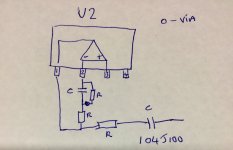
What you are looking for (again assuming all my assumptions are near the mark) would be the equivalent of C2 here.
We do need to investigate that opamp with the incorrect readings because something almost certainly is amiss in that area.
An opamp used in linear mode (such as an amplifier with feedback) will always see the same DC voltage on both inputs. The big question here is whether it is the opamp at fault or the passives around it.
Usually the opamp would be the last suspect and its far more likely to be a component fault around it.
Perhaps some conductivity tests from pin 2 to the surrounding parts would help.
What you are looking for (again assuming all my assumptions are near the mark) would be the equivalent of C2 here.
Attachments
If you are confident working with the SMD chips then you could try lifting just pin 2 from the print (quite easy with a jewellers screwdriver and solder braid) and seeing if the voltage on pin 1 (whatever it ends up as) and the print of pin 2 are now the same.
If so then that would perhaps point to the opamp being faulty rather than a passive dragging pin 2 down.
Another possibility (more unlikely) is that something is feeding a voltage into pin 1 (the opamp output) with enough current ability to exceed the opamps ability to function.
Is the opamp at the same temperature as the others (I think you checked that as I recall).
You could also just swap the opamp although I'm not a believer in doing that without being a lot more certain it is at fault.
I think I can probably lift pin 2 and do the checks. Nothing to loose. Are you suggesting the swapping of U2 and U3? Might have to do this tomorrow though.
If you are confident working with the SMD chips then you could try lifting just pin 2 from the print (quite easy with a jewellers screwdriver and solder braid) and seeing if the voltage on pin 1 (whatever it ends up as) and the print of pin 2 are now the same.
If so then that would perhaps point to the opamp being faulty rather than a passive dragging pin 2 down.
Another possibility (more unlikely) is that something is feeding a voltage into pin 1 (the opamp output) with enough current ability to exceed the opamps ability to function.
Is the opamp at the same temperature as the others (I think you checked that as I recall).
You could also just swap the opamp although I'm not a believer in doing that without being a lot more certain it is at fault.
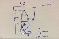
I would normally take Vdd (or Vcc) to be the positive rail. I'm a little puzzled that pin 4 on all the opamps isn't quite at zero although it seems consistent and probably by design (perhaps a ground lift for hum or something).
Your diagram looks electrically correct. The opamp input pins should draw no significant current to pull voltages down. If they do then the opamp is definitely faulty.
Can you see how a leaky cap, the 104J in your diagram, could pull the voltage down.
You can box clever with this to test it with little intervention. You should see 0.0000 volts across the R in series with the cap. If there is DC voltage then the cap is leaky and drawing current.
I think I can probably lift pin 2 and do the checks. Nothing to loose. Are you suggesting the swapping of U2 and U3? Might have to do this tomorrow though.
Swapping parts is the worst possible option tbh, mainly because of the risk of damage and causing other issues. Every possible option should be exhausted before condemning the opamp.
Which R am I checking for current please ?
I need to spend an hour reading Horowitz. I had forgotten that no current flows through the +/- inputs.
I need to spend an hour reading Horowitz. I had forgotten that no current flows through the +/- inputs.
I would normally take Vdd (or Vcc) to be the positive rail. I'm a little puzzled that pin 4 on all the opamps isn't quite at zero although it seems consistent and probably by design (perhaps a ground lift for hum or something).
Your diagram looks electrically correct. The opamp input pins should draw no significant current to pull voltages down. If they do then the opamp is definitely faulty.
Can you see how a leaky cap, the 104J in your diagram, could pull the voltage down.
You can box clever with this to test it with little intervention. You should see 0.0000 volts across the R in series with the cap. If there is DC voltage then the cap is leaky and drawing current.
Attachments
- Status
- This old topic is closed. If you want to reopen this topic, contact a moderator using the "Report Post" button.
- Home
- Source & Line
- Analogue Source
- Phono Pre-amp fault