There are hundreds of DIY phono stage circuits available on the internet, some with component costs of a few $ or €, some for a few thousand $ or €. There are tubes, solid state and hybrid designs, active, passive and active/passive RIAA equalization. So do we need another phono stage circuit? Not really, but they are so much fun to design.
The approach for my new phono stage was the following:
• No feed-back except for local feedback by degradation resistors and thus a discrete circuitry and passive RIAA
• a single-ended design
• battery power supply and hence the necessity of solid state devices (of course also a conventional power supply is possible)
• Cost effectiveness
A no-feedback design requires linear active components. Years ago Nelson Pass wrote in his famous article on cascode amp design:”….in real life, the gain of a transistor, tube or FET changes as the voltage across the devices changes and as the current through the device changes. As these conditions fluctuate, the device creates distortion, but if we hold these conditions to a constant, the device becomes distortionsless.”
In phono preamps tubes can be considered inherently linear as only a miniscule proportion of their voltage swing headroom is used. Hence currents and voltages are kept almost constant, meeting Nelson’s statement. Surprisingly enough high prized tube phono stages (i.e. Allen Wright, K&K Audio or VTA) use a j-FET in their input stages. Modern j-FETs such as the 2SK369 provide very low noise and high transconductance. On the other hand their linearity is poor even compared to BJTs. However, to keep distortion low j-FETs may be selected for a high negative VGS at a desired idle current to achieve current feedback through the source resistor. Cascoding the j-FET with a tube isolates the transistor from the high voltage that allows a high load resistor ensuring sufficient gain (gmFET x Rload) while keeping the j-FET voltage constant and its current change low, a nice approach to merge the advantages of tubes and FETs.
Trying to transfer this concept into the world of transistors is pretty much limited by the maximum voltages of low noise transistors (typically 30 to 50V) excluding the option of high idle currents plus high load resistors. However, a suitable idle current of the j-FET plus a high load resistor can be achieved using a folded cascode design for it allows independent idle currents for the amplifying common source j-FET and the cascoding BJT. A 2SK369 works nicely around 5mA and a BC560 at 1mA. Hence the load resistor value can be multiplied by five compared to a standard common source or cascode design.
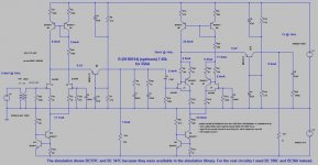
The phono amplifier consists of two amplifying stages, both with single-ended differential designs. The Lundahl LL 9226 step-up transformer is set to a moderate 1:5 turns ratio (termination A in the Lundahl datasheet) to suit my Benz Micro Gold cartridge. Basically it serves two purposes: transforming the tiny 0.4mV signal to a more convenient 2mV and to protect expensive cartridges from being burned by front end failures. Furthermore, the transformer allows a symmetric connection between turntable and preamp if needed. By the way, NEVER use a digital multi-meter to check the transformer wiring for its core may be magnitized permanently (taken from the JAC-Music website).
The two 2sk369 operate at 5.6mA each. A differential design was chosen for the following reasons:
• Cancellation of k2 distortion (although cancellation is not perfect due to different resistor values (R3, R4)in the current mirror)
• Cancellation of idle current fluctuations due to j-FET temperature changes. R23 (as well as R28 in the second stage) ensures similar voltages across both j-FETs and thus similar heat dissipation within the differential pair.
• Higher gain: the second j-FET feeds the signal into the current mirror. The gain of the input stage is around 46db.
The current mirror emitter resistors R3 and R4 are set to 1000 and 1220 Ohm. If J2 feeds 5.6mA into the current mirror, Q3 sources a total of 6.8mA. J1 takes 5.6 mA leaving 1.2 mA idle current for the cascoding Q2. R4 may need some tweaking to adjust the idle current of Q2 to 1.2 mA. R6 and R7 set the drain of Q2 to 9.3V. The oscilloscope showed a better square wave response when both resistors were bypassed with capacitors. The gate resistor of J2 is equal to the copper resistance of the LL9226 secondary coils. Again C3 improves square wave response.
The RIAA network simply is a frequency dependent load of the cascoding Q2 lacking the typical voltage dividing first resistor of conventional passive RIAA networks. Thus the RIAA network impedance controls the gain without any component in the primary signal path.
The basic configuration of the second stage is identical to the first. The pair of j-FETs in the first stage is replaced by two Sziklai pairs comprising a j-FET and a bipolar transistor again with the scope to minimize current changes in the j-FET transistors. Idle currents are higher to suit the 1k resistor at the collector of Q10. Q4, Q9 and Q10 may require some cooling because of the elevated idle currents.
Any comments are greatly appreciated I will provide pictures shortly
The approach for my new phono stage was the following:
• No feed-back except for local feedback by degradation resistors and thus a discrete circuitry and passive RIAA
• a single-ended design
• battery power supply and hence the necessity of solid state devices (of course also a conventional power supply is possible)
• Cost effectiveness
A no-feedback design requires linear active components. Years ago Nelson Pass wrote in his famous article on cascode amp design:”….in real life, the gain of a transistor, tube or FET changes as the voltage across the devices changes and as the current through the device changes. As these conditions fluctuate, the device creates distortion, but if we hold these conditions to a constant, the device becomes distortionsless.”
In phono preamps tubes can be considered inherently linear as only a miniscule proportion of their voltage swing headroom is used. Hence currents and voltages are kept almost constant, meeting Nelson’s statement. Surprisingly enough high prized tube phono stages (i.e. Allen Wright, K&K Audio or VTA) use a j-FET in their input stages. Modern j-FETs such as the 2SK369 provide very low noise and high transconductance. On the other hand their linearity is poor even compared to BJTs. However, to keep distortion low j-FETs may be selected for a high negative VGS at a desired idle current to achieve current feedback through the source resistor. Cascoding the j-FET with a tube isolates the transistor from the high voltage that allows a high load resistor ensuring sufficient gain (gmFET x Rload) while keeping the j-FET voltage constant and its current change low, a nice approach to merge the advantages of tubes and FETs.
Trying to transfer this concept into the world of transistors is pretty much limited by the maximum voltages of low noise transistors (typically 30 to 50V) excluding the option of high idle currents plus high load resistors. However, a suitable idle current of the j-FET plus a high load resistor can be achieved using a folded cascode design for it allows independent idle currents for the amplifying common source j-FET and the cascoding BJT. A 2SK369 works nicely around 5mA and a BC560 at 1mA. Hence the load resistor value can be multiplied by five compared to a standard common source or cascode design.
The phono amplifier consists of two amplifying stages, both with single-ended differential designs. The Lundahl LL 9226 step-up transformer is set to a moderate 1:5 turns ratio (termination A in the Lundahl datasheet) to suit my Benz Micro Gold cartridge. Basically it serves two purposes: transforming the tiny 0.4mV signal to a more convenient 2mV and to protect expensive cartridges from being burned by front end failures. Furthermore, the transformer allows a symmetric connection between turntable and preamp if needed. By the way, NEVER use a digital multi-meter to check the transformer wiring for its core may be magnitized permanently (taken from the JAC-Music website).
The two 2sk369 operate at 5.6mA each. A differential design was chosen for the following reasons:
• Cancellation of k2 distortion (although cancellation is not perfect due to different resistor values (R3, R4)in the current mirror)
• Cancellation of idle current fluctuations due to j-FET temperature changes. R23 (as well as R28 in the second stage) ensures similar voltages across both j-FETs and thus similar heat dissipation within the differential pair.
• Higher gain: the second j-FET feeds the signal into the current mirror. The gain of the input stage is around 46db.
The current mirror emitter resistors R3 and R4 are set to 1000 and 1220 Ohm. If J2 feeds 5.6mA into the current mirror, Q3 sources a total of 6.8mA. J1 takes 5.6 mA leaving 1.2 mA idle current for the cascoding Q2. R4 may need some tweaking to adjust the idle current of Q2 to 1.2 mA. R6 and R7 set the drain of Q2 to 9.3V. The oscilloscope showed a better square wave response when both resistors were bypassed with capacitors. The gate resistor of J2 is equal to the copper resistance of the LL9226 secondary coils. Again C3 improves square wave response.
The RIAA network simply is a frequency dependent load of the cascoding Q2 lacking the typical voltage dividing first resistor of conventional passive RIAA networks. Thus the RIAA network impedance controls the gain without any component in the primary signal path.
The basic configuration of the second stage is identical to the first. The pair of j-FETs in the first stage is replaced by two Sziklai pairs comprising a j-FET and a bipolar transistor again with the scope to minimize current changes in the j-FET transistors. Idle currents are higher to suit the 1k resistor at the collector of Q10. Q4, Q9 and Q10 may require some cooling because of the elevated idle currents.
Any comments are greatly appreciated I will provide pictures shortly
Attachments
I hope that you are referring a Linear systems LSK389 part which is in production. Why not try that mfg model in your sims to see if it makes any difference to what ever model you are using for a 2sk389. I do not believe that Toshiba ever released a spice model of their 2sk389, have to wonder where the models came from and if anyone verified them.
Good luck in your MC phono amp design. It is always nice to see new design concepts
Wonder what that transformer costs? MC phono setups are expensive to say the least. I am sure that cartridge ain't cheap either")
Good luck in your MC phono amp design. It is always nice to see new design concepts
Wonder what that transformer costs? MC phono setups are expensive to say the least. I am sure that cartridge ain't cheap either
...
Any comments are greatly appreciated I will provide pictures shortly
Hi!
fine design!
please send asc file,
thank you in advance!

Thanks for your comments. The spice model is for 2SK369. I found it somewhere on the internet, no idea whether the model is authorized by Toshiba. However, the model nicely matches the specifications from the 2sk 369 datasheet and the LT SPICE model simulations closely correspond to the real life measurements.
Input Miller capacitance is a problem in conjunction with step-up transformers. For that reason a cascoded input design was chosen that limits the 2sk369 input capacitance to its static gate capacitance despite a high gain of the input stage for the drain sees no voltage change.
Enclosed I added the *.asc file that corresponds to the schematic above.
Cheers
KlausB
Attachments
When using a step-up, be very careful about the loading of the secondary, especially with an input stage having significant Miller capacitance. This is an issue almost always ignored and that (IMO) is what gave step-ups a poor reputation.
Very true!
Input Miller capacitance is a problem in conjunction with step-up transformers. For that reason a cascoded input design was chosen that limits the 2sk369 input capacitance to its static gate capacitance despite a high gain of the input stage for the drain sees no voltage change.
Cascoding helps, but you'll still need to use a Zobel across the secondary to optimize things. This should be done experimentally using a source impedance equalling the cartridge's DCR.
Thx for the sim
Sorry, I got 2sk389 mixed up with 2sk369, but the same applies, it is an obsolete part that not everyone can obtain.
As for the bc550c/560c models you can get them from Bob Cordell's web site or I will post them here for you
.MODEL BC550C npn IS=45e-15 BF=689 VAF=162 IKF=0.09 ISE=4600e-15 NE=2 NF=0.9965 RB=167 RC=1 RE=0.04 CJE=18.7e-12 MJE=0.35 VJE=0.75 CJC=6.2e-12 MJC=0.25 VJC=0.4 FC=0.5 TF=595e-12 XTF=10 VTF=10 ITF=1 TR=10e-9 BR=12.2 IKR=0.34 EG=1.2 XTB=1.65 XTI=3 NC=0.996 NR=1.0 VAR=120 IRB=7e-5 RBM=1.1 XCJC=0.6 ISC=5e-15 mfg=CA030111
.MODEL BC560C pnp IS=60e-15 BF=900 VAF=160 IKF=0.10 ISE=70e-15 NE=1.42 NF=1 RB=170 RC=1.0 RE=0.05 CJE=19e-12 MJE=0.3 VJE=0.75 CJC=3.9e-12 MJC=0.3 VJC=0.75 FC=0.5 TF=600e-12 XTF=7 VTF=4 ITF=0.45 TR=10e-9 BR=3 IKR=0 EG=1.1 XTB=1.5 XTI=3 NC=2 ISC=0 mfg=CA030211
Oops, I did not know that 2SK369 is obsolete. Over here they are still available at
2SK-Transistoren bei reichelt elektronik
Thanks a lot for the models. I will try to fit them into my simulation.
A folded cascode basically has the same effect as the "standard" cascode on the input transistor. The drain (or collector or anode) voltage is kept constant and thus the Miller capacitance eliminated. A folded cascode requires NPN and PNP devices which makes its implementation difficult in all tube designs but it is a really nice approach to expand your voltage swing in solid state designs.
I have to think about the zobel network.
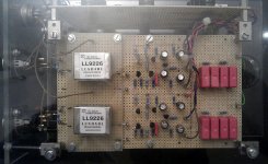
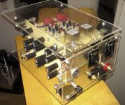
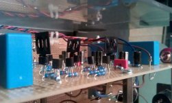
Here are some pictures.
2SK-Transistoren bei reichelt elektronik
Thanks a lot for the models. I will try to fit them into my simulation.
A folded cascode basically has the same effect as the "standard" cascode on the input transistor. The drain (or collector or anode) voltage is kept constant and thus the Miller capacitance eliminated. A folded cascode requires NPN and PNP devices which makes its implementation difficult in all tube designs but it is a really nice approach to expand your voltage swing in solid state designs.
I have to think about the zobel network.
Here are some pictures.
Attachments
Hi,
don't expect that Reichelt has any stock left (they also list the SK170 and other long since obsolete JFETs)
They've been informed multiple times about those errors and still haven't corrected for in their catalogue.
You may think about the BF862 (NXP) as improved replacement, or the 'clones' for SK170, SK389, SK147 etc from small specialist companies like LinearSystems, Calogic or Interfet.
jauu
Calvin
Last edited:
Does a "folded cascode" provide similar benefits to a conventional cascode for input capacitance?
Yes, it does. Both have the same AC circuit model.
Last edited:
Hi,
hacked the circuit into LTSpice again to simulate advanced features.
Klaus, are you sure about the parameters of the Input tranny?
With the given values (250H for L2) the bandwidth is grossly limited to ~7.4kHz culminating in a loss of -10.6dB @20kHz.
L2=100H would result in -3dB@20kHz with an approximately -4dB lower gain.
A set of L1/L2 of 4H/100H restores the former gain, increasing the lower bandwidth only slightly.
Noise over 20Hz-20kHz is a bit high at around -65dB.
A point that I wondered about from the fisrt moment I saw the circuit.
Differential input and active current mirror loads are certainly not the lowest noise designs.
The idea of using a folded cascode and hence to control the idle currents through the input- and the cascoding device separately, could easily be achieved with a singleended input and a resistor in place of the current mirror Q3/Q1.
The anyway high positive supply line would allow for increased Drain load resistors ... using the active CMs the positive supply line could be as low as the negative supply line, hence +12V.
Attached are the sim-file and models of the BC550C and BC560C after Cordell, as well as Zetex medium power transistors FZT651 and ZT751, which may be a (probabely even improved) replacement for the BCs as cascode devices.
Also included are the models of the BF862 from NXP and the LSK389 A/B/C from Linear Systems and the Cordell model of LSK389C (which is actually a LSK389B, Idss-wise)
jauu
Calvin
Attachments
Last edited:
Hi Calvin,
thanks a lot for putting so much effort in that circuitry. Unfortunatey Lundahl does not provide any information on the inductances of his LL9226 step-up transformer. I chose the inductances in that schematic arbitrariliy, just to simulate the 1:5 step-up process. Probably the values are far, far away from the real life transformer. Sorry for that confusion.
Your comments and suggestions on a single ended input stage:
I tested a similar design. It works very nice in the simulation. The problem in real life is the high temperature sensitivity of the j-FETs. Even if you just touch the FET with your finger, the current starts to float. Any current change of the j-FET input transistor enforces the same current change in the cascoding transistor. The idle current of the latter one is only 1/5 of the FET's idle current and with the relatively large load resistor of 8k the point of operation is floating at an unacceptable extent with temperature changes.
Hence one of the main purposes of the second FET is the cancellation of current changes due to temperature changes.
Regards
KlausB
Attachments
'clones' for...SK147...from small specialist companies like LinearSystems, Calogic or Interfet.
Which would that be ?
The problem in real life is the high temperature sensitivity of the j-FETs.
KlausB, you can always try to bias Jfets at their zero tempco, which is
-Vgoff+0,6V
Best,
This Vgoff +0.6V is Borbely's figure.KlausB, you can always try to bias Jfets at their zero tempco, which is
-Vgoff+0,6V
Best,
I doubt it is accurate.
I go further. It is wrong.
Read the Siliconix book/app notes by Ed OxnerThis Vgoff +0.6V is Borbely's figure.
I doubt it is accurate.
I go further. It is wrong.
- Status
- This old topic is closed. If you want to reopen this topic, contact a moderator using the "Report Post" button.
- Home
- Source & Line
- Analogue Source
- Do we need another phono stage?