Thanks you for that. It proves that the 0.6V or 0.65V are both wrong.
Look at the example.
The zero temperature effect is @ 0.85Vgs.
Add on 0.6V to get 1.4Voff or 0.65V to get 1.45Voff
You will find when you measure the 1.4mA Idss device, that Vp (Voff) is much higher than 1.4V or 1.45V. Probably somewhere between 1.6V and 2V.
Look at the example.
The zero temperature effect is @ 0.85Vgs.
Add on 0.6V to get 1.4Voff or 0.65V to get 1.45Voff
You will find when you measure the 1.4mA Idss device, that Vp (Voff) is much higher than 1.4V or 1.45V. Probably somewhere between 1.6V and 2V.
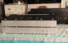
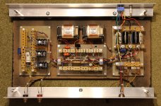
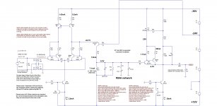
The next generation
The successor of the phono stage I started this thread with again is a discrete no-(global)feedback concept but with BJTs only in the direct signal path. It will comprise one single gain stage that amplifies the MC signal to line level, followed by a passive RIAA equalization and a subsequent emitter follower at the output. A step-up transformer elevates the MC signal close to MM level.
A Lundahl LL1933 step-up transformer multiplies the MC output voltage by the factor eight. The two dual input low noise transistors 2N3810 (PNP) and MAT 12 (NPN) are connected in a Sziklai configuration. The current distribution through both transistors is determined by the ratios of the resistors R17/R18 and R19/R21.The current mirror has a 1:6.5 ratio. Q7 is a folded cascode drawing an idle current of 7.9mA. Its current is fed into the passive RIAA. The requested high gain of the input stage requires a high load impedance at the collector of Q7. The 21k resistor (R14) alone would limit the collector current to a value below 1mA with respect to its voltage drop. This would severely compromise the overload capability of the input stage. Therefore a choke is in parallel with the 21k resistor. Its inductance is 810H, its copper resistance is 2.4k. Thus the DC load at the collector of Q7 is 2.4k in parallel with R14 while the AC load is almost 21K at the low end of the audio spectrum which then decreases with ascending frequency according to the RIAA equalization curve. The second stage is just an impedance converter with unity gain. The PNP/NPN Sziklai pair input impedance is of several Megohm at the base of the transistor Q23. The p-channel MosFet on top is configured to bootstrap the transistors. Thus the emitter / collector voltage across the Sziklai transistors is kept constant to reduce distortion.The maximum voltage swing of the phono stage is above 30Vpp before clipping.
Attachments
- Status
- This old topic is closed. If you want to reopen this topic, contact a moderator using the "Report Post" button.