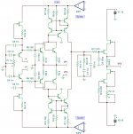
Here is the two stage approach. The BJT version can be modified in the same way so we have our 4 versions :
1 : Fet High Z AIOG
2 : Fet High Z Two Stage
3 : BJT Low Z AIOG
4 : BJT Low Z Two Stage
So lets call them MPP2011 1.0
MPP2011 2.0
MPP2011 3.0
MPP2011 4.0
for simplicity. If we make any changes or improvements we just call them 1.1, 1.2 etc.
When you ask me what i like better, AIOG or Two Stage i would say they have equal merit. The AIOG is simpler so potentially more transparent and the Two Stage has higher dynamic range and lower distortion, not that the AIOG has high distortion in the first place.
Attachments
Thank you for your efforts.It is the first time I have noticed that you are not giving all the components details. Circuits are probably the most complex phono stages I have ever seen. Are they very low noise? They use single complementary transistors, without usual paralleling.Here is the two stage approach. The BJT version can be modified in the same way so we have our 4 versions :
1 : Fet High Z AIOG
2 : Fet High Z Two Stage
3 : BJT Low Z AIOG
4 : BJT Low Z Two Stage
So lets call them MPP2011 1.0
MPP2011 2.0
MPP2011 3.0
MPP2011 4.0
for simplicity. If we make any changes or improvements we just call them 1.1, 1.2 etc.
When you ask me what i like better, AIOG or Two Stage i would say they have equal merit. The AIOG is simpler so potentially more transparent and the Two Stage has higher dynamic range and lower distortion, not that the AIOG has high distortion in the first place.
In fact you can use up to 4 pairs on each side in the Fet version. I have drawn with only one pair for clarity. With one pair you get 0.7nVq/Hz with two pais 0.5nVqHz and with 4 pair you get 0.3nV/qHz, then effects set in that prevent an even better result . That is 3dB, 6dB and around 10dB better then an AD797 so they all qualify as low noise. The BJT version is 0.5nV/qHz with one pair and 0.3nV/qHz with two pairs. It has higher transconductance ( BJTs have around 10x the Gm of Fet stages with the same idle current ) and lower 1/F noise so the open loop gain is higher and the bass is less noisy. Subjectively noise is about similar because the ear looses sensitivity in the lower reaches where 1/F noise sets in in Fets.
This has all being beaten to death here many time but i understand that you do not follow each and every post. Anyway, i will start with version 1 and we will see a full schematic soon.
This has all being beaten to death here many time but i understand that you do not follow each and every post. Anyway, i will start with version 1 and we will see a full schematic soon.
The JLH Homage JG is progressing slow. First i made a mistake. The transdiodes conduct as much current as the input transistors and also there are 4 mA flowing in the feedback resistors so the output transistors where starved because the voltage over the collectors
of the input transistors dropped accordingly. I have fixed that. I also had a strange idea to bring down the DC offset at the output. I simply revered the transdiodes so that the P channel is working on the N channel and vise versa. That dropped the Dc offset to 50mV.
I also will insert a potmeter and try to trim the offset further that way. I start to understand better this simple circuit. There is a lot of entanglement going on here so it is not that simple in detail.
Attachments
After mucho experimenting i come to the conclusion that the original JLH circuit is the best compromise. With my version there is a DC offset problem i can not solve easy at the moment and a 3dB noise penalty because of the transdiodes in series with the signal. That is a too high cost for the advantage of DC coupling i think. I can lower the noise of the original circuit though by using higher currents, better transistors and lower value feedback resistors. That requires a higher value elcaps. I do not see the reliability problem if good quality caps are used like Rubicon ZL.. Pannasonic FM, FC, Nichcon KZ Muse or the superior Elna Silmic 2. I will draw the circuit how i whould build it and then move on to a DC coupled circuit that does not have some of the problems of this one. It is the Piglets Dad Crophead, made for Tac McLaren. This is now double differenntial so one step up on the ladder for parallel symmetric amps.
So how is DC feedback made easier ? Simply by using a differential amplifier. See Piglets Dad MC design. PSSR is not great in that design so i would use constant current sources.
Idle current in the input stage is 3mA so this is closer to what i would use. The disadvantage again is a 3dB noise penalty because the input transistors are in series.
That is the reason i arrived at parallel symmetric designs like MPP2011 1.0 to MPP2011 4.0.
Idle current in the input stage is 3mA so this is closer to what i would use. The disadvantage again is a 3dB noise penalty because the input transistors are in series.
That is the reason i arrived at parallel symmetric designs like MPP2011 1.0 to MPP2011 4.0.
Attachments
Where do we move on from here ? As i said, i arrived at parallel symmetric. That is where the Fets come in. They are "self biasing" and do not have the DC offset problem into the cartridge. The most simple version would be A. This has better PSSR then Piglets Dads because the Fets work as a constant current source. A better way is B, not much different then a Vendetta. Here the second stage is a folded cascode , giving much better speed.
I build many nice phonos that way. A good example is the MPP FF2010 you can see earlier in this thread. Since then i have moved on to current mirrors and other more advanced stuff but when you need a quick fix, version B is a very good start. Version A and B can be build with bipolars at the input when you solve the biasing problem and the input offset if you are afraid of that. The second stage can be Mosfets. Vertical or better lateral. I have shown all this before. Now you understand that the JLH is only interesting on an historical basis and i have no motivation to max it out any more. It´s good, very good, and costs nothing but i prefer my latest designs. They are more quiet, higher speed, less distortion, higher dynamic range, better PSSR and so it goes.
I build many nice phonos that way. A good example is the MPP FF2010 you can see earlier in this thread. Since then i have moved on to current mirrors and other more advanced stuff but when you need a quick fix, version B is a very good start. Version A and B can be build with bipolars at the input when you solve the biasing problem and the input offset if you are afraid of that. The second stage can be Mosfets. Vertical or better lateral. I have shown all this before. Now you understand that the JLH is only interesting on an historical basis and i have no motivation to max it out any more. It´s good, very good, and costs nothing but i prefer my latest designs. They are more quiet, higher speed, less distortion, higher dynamic range, better PSSR and so it goes.
Attachments
Stage A and B can also be build with negative feedback. As drawn they have feedback too but local current feedback that some people call zero feedback. That is not true. A working stage with stable parameters can not be build without feedback. Feedforward or better error correction is an option but mathematically it is possible to express feedforward as a special case of feedback too. As i said many times, it is not so much the topology, it is the execution. That makes it so difficult to me to recommend "the best" stage. For beginners the Nobrainer is a very cool solution and when you want what is technically possible build the FPS from Pilgham. If that does not suit you follow the process and learn. All the others have already found nirvana.
After my little tutorial on parallel symmetric design i went back to the MPP Summer 2011 1.
I think this circuit deserves a PCB and also to be build and listened too. Maybe i can persuade Jan Didden to do the layout or somebody else from here can do it. I put now most of the component values and types into the circuit. The Fets that provide constant current to the Leds can also be substituted with resistors as long as 1 - 4mA flow in the Leds without much disadvantage. I have drawn only one Fet and Led per type but actually 4 of each are needed. I have not dimensioned the Gyrators. That can be a simple BJT cap multiplier like the one used by B.Vogel ( it works well, i tried it ), a Fet multiplier JC style, an Opamp multiplier, a mixture or simply an RC combination that can sound good too. The circuit could even be supplied from the DC direct because the mirrors have excellent PSU rejection.
I think this circuit deserves a PCB and also to be build and listened too. Maybe i can persuade Jan Didden to do the layout or somebody else from here can do it. I put now most of the component values and types into the circuit. The Fets that provide constant current to the Leds can also be substituted with resistors as long as 1 - 4mA flow in the Leds without much disadvantage. I have drawn only one Fet and Led per type but actually 4 of each are needed. I have not dimensioned the Gyrators. That can be a simple BJT cap multiplier like the one used by B.Vogel ( it works well, i tried it ), a Fet multiplier JC style, an Opamp multiplier, a mixture or simply an RC combination that can sound good too. The circuit could even be supplied from the DC direct because the mirrors have excellent PSU rejection.
Attachments
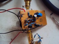
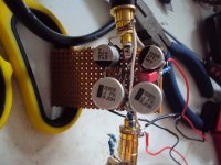
I have finished now building the JLH JG in the elcap version and it works just fine. I also found out why my DC coupled experiments failed. I had connected the collector of one output transistor in a wrong way so i was running that thing on single ended. It did amplify though and that confused me. Feel free to try the DC coupled versions if you wish. I will stop here for the time being. I got it to lower noise and i am happy with that.
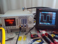
I made some measurements on the JLH JG. Idle in the input stage is 6mA and 17mA in the output stage. Amplification factor is x30 with a 5.1 Ohm feedback resistor. The output transistors can drive 17mA x 300 Ohm = 5.1 V in class a so this circuit will not leave class a any time soon. Bandwidth is 500kHz with a 150pF compensation cap. 10kHz square wave
looks good. I use 2 x 9V blocks for supply. Under this conditions the voltage is plus-minus 6V after the 80 ohm resistors. DC offset at the input is 70uV measured with a precision meter, that is under my 100uV criterion. Here the rather high Hfe of the Hitachi transistors helps although i run the stage on 4 times the current of the original JLH. See some pictures. I could keep the size compact by using 3900uF/9V Pannasonic SMD elcaps. The caps measure 30mOhm impedance at 100kHz. When i started building at the age of 11 a 10.000uF cap with 35V had the size of a cola can. We have come quite far in the meantime.
looks good. I use 2 x 9V blocks for supply. Under this conditions the voltage is plus-minus 6V after the 80 ohm resistors. DC offset at the input is 70uV measured with a precision meter, that is under my 100uV criterion. Here the rather high Hfe of the Hitachi transistors helps although i run the stage on 4 times the current of the original JLH. See some pictures. I could keep the size compact by using 3900uF/9V Pannasonic SMD elcaps. The caps measure 30mOhm impedance at 100kHz. When i started building at the age of 11 a 10.000uF cap with 35V had the size of a cola can. We have come quite far in the meantime.
Attachments
I posted more then i wanted the last days. I am alone at home. The family is in vacation.
When i get lonesome i land on the web usually. Maybe too many posts for some that have lost the guiding line again. As i said many posts ago my intention is not so much to bring up a "best" recipe but show the process of how things come together and happen in my place. Including mistakes and dead ends. Anyway, i have to keep a promise. Show you the zero impedance balanced transimpedance stage. Actually i would call it a balanced complimentary compound stage. It was designed by Smedegaard when he was at Becker Automotive as an I/V converter in a DA converter. I have not seen it used though so it is somewhat obscure. Many I/V stages can be used as MC input stages. Malcolm Hawksford told me that 20 years ago and also the engineering challenge is not that different. Low noise, high speed, low distortion etc.
So please look at the concept. I will elaborate later.
Attachments

The circuit post 2537 may not work the way i have drawn it. Take away the plus and minus signs ( thanks AS ) . How the input could be configured is open to discussion.
Maybe it is totally useless for our purpose but who knows. Does anybody have a working idea ? For your degustation, here is the original article.
http://www.linearaudio.nl/Miscellaneous/smedegaard 4217 aes pp.PDF
Maybe it is totally useless for our purpose but who knows. Does anybody have a working idea ? For your degustation, here is the original article.
http://www.linearaudio.nl/Miscellaneous/smedegaard 4217 aes pp.PDF
Thank you for this PDF file.
The circuit, Fig. 34 (p. 25) in this text, is a little bit different from what
was shown in post 2537, it has a summing function for the output of
two DA-converters. The outputs are offset by a single Ube drop each.
Fig. 24 (p. 20) is also interesting and has no input offset.
Both circuits are non inverting, the inverting inputs being grounded.
Last edited: