I'm cheking my Phono for RIAA Accuracy and Gain with a Generator and Osciloscope
RIAA with Osciloscope measurement looks fine with some exception on the range above 15Khz which seems to offset more than 2db, maybe a measurement error, I do not know..
Another issue is that my Output trace does not look nice over 15Khz and seems to "oscilate" on a 2-3Hz period, That begins early on the spectrum at around 500-800Hz and getting worse as the frequency raise.
Below I have two small Videos of the Oscilloscope at 5Khz and 15Khz.
Have in mind that my phono is in a cartoon box, so some noise from the enviromment is probably there
Generator is set at 600mV divided by Voltage divider (62KOhm & 120Ohm to Ground) so an 1mV input to Phono
Any opinions?
YouTube
YouTube
Lab gen & scope of moderate cost can add significant error when looking to resolve below a couple of dB accurately. But a sure thing is you miss C2Y in your build photos for now.
For the other thing I can't understand what you mean exactly and I can't see any videos, the links don't give something. Try more level, RIAA cuts 20dB in the highs, maybe you miss sufficient signal for the scope to trigger.
For the other thing I can't understand what you mean exactly and I can't see any videos, the links don't give something. Try more level, RIAA cuts 20dB in the highs, maybe you miss sufficient signal for the scope to trigger.
Hi Salas, Is there a circuit description for the FSP like the DCG3 thread post #47?
I’ve been trying to better understand how this circuit works. I’m loving this project and very happy I’m finally getting back into the hobby.
Many thanks as always, for all your knowledge and support
Ps: I’m slowly getting through the 1600 + pages of this thread.

Not a special post that I remember of. It is explained in much detail of course but not like a presentation because it morphed as the thread continued. So it was understood just by dialogue about its various bits as the developments and builds went on.
Measure with different Ref 1kHz for half down and half up the spectrum so to can contain better the 40dB opposite curve extremes. Because if you will use much signal to improve the SNR of the casual measurement loop in the highs VS 50HZ interference modulation, same ref signal level will clip the lows.
Measure with different Ref 1kHz for half down and half up the spectrum so to can contain better the 40dB opposite curve extremes. Because if you will use much signal to improve the SNR of the casual measurement loop in the highs VS 50HZ interference modulation, same ref signal level will clip the lows.
If I understand well you tell me to have the 1mV let say for 1khz and below
and to raise the input for measure the 1khz and up, what input reference you suggest for the second?
If I understand well you tell me to have the 1mV let say for 1khz and below
and to raise the input for measure the 1khz and up, what input reference you suggest for the second?
Yes. Double, triple, or more. Whatever helps your reading stability in the HF before clipping it.
You were watching an old black and white comedy with Stavridis by the way? I thought I listened to one of his classic punch lines in the background "and I will eavesdrop and I will peep away"
Yes I did, I'm a big fun of old B&W Cinema
Hi Salas, Is there a circuit description for the FSP like the DCG3 thread post #47?
I’ve been trying to better understand how this circuit works. I’m loving this project and very happy I’m finally getting back into the hobby.
Many thanks as always, for all your knowledge and support
Ps: I’m slowly getting through the 1600 + pages of this thread.
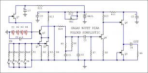
So here is a rather concise explanation of the FSP schematic in a single post. I hope it will be helpful to more members. We will not go into the whys of its topological and parts choices philosophy here. Just to the mechanics. Its a two gain stages plus buffer architecture discrete preamp. Lets see the stages one by one.
A. Input stage
The phono cartridge's signal goes through a switched loading choice system and its applied to the gates of Q1 & Q2 minimal noise type JFETS. Cooperating with Q3 BJT the stage's gain engine is formed. Q1 & Q2 are a common source amplifier while Q3 is a common base one that sits on their drains in series. The common base part shields the JFETS transcondactance from the load resistor R4. The technique is called "cascode" and its goal is not to let their gate to drain parasitic capacitance magnify more than a couple of times while the signal is still amplified to high gain by this JFET+BJT combination system. Else the total input referred capacitance would have escalated at same amplification rate as the signal's. Such capacitance boost is called Miller. We don't want it here. It brings various negative effects regarding proper cart loading, electrical resonance, bandwidth limiting. Especially for MM cartridges.
This cascode is also a kind that goes around to the ground point for reference than going up to the rail. Q3 is PNP while R4 loads it and folds over to GND. That is why its called a folded cascode. The much more common type that refers to the rail is called telescopic. It must still draw current from a power source nonetheless so R13 provides it as passive CCS. DC current flows through Q1 Q2 and R2 R3 to ground. They ask for a certain amount as a system dependent on IDSS and degeneration. What is surplus goes through Q3 to R4. It creates a collector output DC voltage we want to keep at about half the value where Q3's base sits. Q7 is a JFET CCS that sends current to D1-D4 LEDS creating with their VF a steady DC voltage point for Q3's base. C8 filters for noise. Across R4 the output signal develops by the action of Q3. R12 and R15 make proper DC drops in the circuit. C6 & C7 form local filters with those.
Rail voltage value, R12//VR1, R13, Q1 Q2 IDSS, R2 R3, all form a balance system which is both pre-calculated and trimmer adjustable to set the two bias currents of the cascode combo in correct analogy. To monitor and adjust the resulting DC voltage difference between Q3's base and collector, test points are marked on the PCB (TP1 TP2). The PSU's variable output voltage setting adjusts the system while VR1 lends a finer touch if needed.
B. RIAA and the second stage
There is no negative feedback loop between stages in this preamp so it can't nest some interstage active filter. A passive RIAA filter network of no "lost constant" addition is located between stages one and two. R14 R5 C1 C2 form its base impedance and LF/HF filter curve branches. R6 is corrective to R5's standard value, makes it more precise, or a special value R5 can be used skipping R6. There is also a C2Y pF range capacitor place on the PCB to complement C2's value against tolerances or towards preference. They are the important HF branch. Both the input stage's source impedance and the second stage's Miller effect have been included in the total filter's tuning. C3 AC couples the equalized signal to stage two. R7 refers Q4 JFET's gate to ground. R10 is its drain load and R8 is its source degeneration providing some judicial amount of local feedback to better THD. This single high transconductance JFET common source stage is potent enough for further amplifying to the final output voltage swing goal. Aiming at 300-400mV AC RMS with most cartridges. As recommended for LMC/MC/HMC/MM nominal output ranges and the circuit's proper sensitivity configuration options in the build manual. The DC level created between R10 and Q4's drain is also the voltage reference point for the output buffer circuit.
C. Output buffer
Q6 copies the signal as seen at its gate while performing current gain only. It is a source follower. Through C4 AC coupling the buffered signal finally outputs. There are no degeneration or damping resistors. Thus the output impedance is no more than the intrinsic RDS. Usually 30-50 Ohm for this JFET type. Q5 is configured as an IDSS current source and determines the current bias of Q6. R9 provides a local discharge path to C4 not to suddenly do it when connecting gear. R11 and C5 form an RC filter for proper voltage drop to center the buffer in regard to Q6's gate voltage bias. It also performs some local noise cleaning.
I hope it was a simple enough description to follow. I linked it in post#1 too. For the FSP's integrated PSU please refer to the BIB SSLV1.1 shunt regulator as they are highly related. The SSLV1.1 build thread
Attachments
Salas, I will give it a try. Thanks again.John try 18 Ohm R2 source resistor to your 10mA IDSS K369 Q1 input stage along with a 3.3K 1W R13. Q2 R3 not populated. You should get the middle ground 50dB gain you require.
Thanks for that concise description. It is a wonderful circuit and I have been enjoying it for years. Life has kept me too busy for audio projects for some time and I have to admit your Salas Folded has been sitting on a piece of plywood by the turntable for a looooong time. Life is sorting out and I finally have some spare time. I pulled the partly finished chassis out of storage and have been enjoying working on it in my spare time the last few weeks. Your description of this wonderful phono preamp reminded me about why I chose to make it. Makes finishing it even more rewarding.
Thanks
Jim
Thanks
Jim
Thank you so much! You really are an amazing person. Your effort to help others is inspiring.
I’m a chef with a desire to better understand audio electronics, you’ve never met me, but whenever I ask for assistance you’re there. Where do I send the wine?
I’m waiting on parts, so plenty of reading for me. Such an amazing amount of knowledge in this thread as in others also.
Thanks Legend
I’m a chef with a desire to better understand audio electronics, you’ve never met me, but whenever I ask for assistance you’re there. Where do I send the wine?
I’m waiting on parts, so plenty of reading for me. Such an amazing amount of knowledge in this thread as in others also.
Thanks Legend
Last edited:
There can be some adjustment of resistor values to recommend for your intermediate target gain. But first I need to know your cartridge model and the IDSS of the K369 you have installed.
I think I would be interested in the same for my build. Cartridge is an AT ML440MLa. The K369 Idss I'd have to look at but think they are in the 11-12mA range. Intended loading will be ~33K. The cartridge is spec'd at 4mV output. Calculation results in ~48dB (log(1/.004)*20).
And most appreciate all of your work on this, and recently the discussion of measuring/selecting the LEDs using Q7.
Can't wait to listen to this; Thorens TD320 has been in storage far too long
- Home
- Source & Line
- Analogue Source
- Simplistic NJFET RIAA