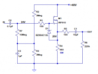
I have some IRF510 MOSFETs sitting in a drawer which I'd like to use to make simple source followers to buffer a high-ish impedance signal source to a pair of powered speakers with low-ish 10k ohm input impedance.
Does this look like a viable circuit (attached)?
Is this 'silent bias' voltage divider scheme going to work biasing an enhancement-mode MOSFET? Or will the MOSFET fail to turn on?
I also have a few IRF630 MOSFETs. Would those perform better in this usage than IRF510? Or is there practically no difference between the two types?
I'm almost completely naive to working with transistors, hence the beginner questions.
Thanks for any advice.
--
Attachments
Hi , according to irf510 datasheet , input capacitance is 180pf , it may have shunting effect on high frequencies and with high impedance sources. But it should work . What will be input signal amplitude? If line level ,such high supply voltage not needed , 12-15v would be sufficient I think.
The Cgd = Crss (which decreases with increasing drain-source voltage) directly loads the input, the Cgs = Ciss - Crss is largely bootstrapped out because the source voltage more or less follows the gate voltage. It follows more accurately with a current source than with a resistor, so current source biasing will also reduce the input capacitance to some extent.
Given similar processing (IDK whether these p/n's are 'same generation' or not), the lower voltage / lower current '510 would give somewhat better performance due to its lower parasitic capacitances.
Both are massively over-spec'ed for this task and would easily be bettered by a long list of alternative p/n's. But you have 'em, so why not? -- go for it!")
And yes, definitely lower the supply voltage -- +1 ximikas
Just how sure are you that you need this buffer? If its just a fun project to put a couple IRF510's to work, it will probably satisfy. But 10k isn't usually considered to be a low impedance input; and if your source impedance really is high, it will have a high frequency roll-off trying to drive a big MOSFET's input capacitance (which is what you have).
Cheers
Both are massively over-spec'ed for this task and would easily be bettered by a long list of alternative p/n's. But you have 'em, so why not? -- go for it!
And yes, definitely lower the supply voltage -- +1 ximikas
Just how sure are you that you need this buffer? If its just a fun project to put a couple IRF510's to work, it will probably satisfy. But 10k isn't usually considered to be a low impedance input; and if your source impedance really is high, it will have a high frequency roll-off trying to drive a big MOSFET's input capacitance (which is what you have).
Cheers
Last edited:
Thanks everybody!
Good to know I understand the basic idea behind biasing the enhancement mode N-channel MOSFET with a voltage divider. I was afraid since an enhancement mode device is normally off, it would take more than a voltage divider feeding the correct voltage to the gate to get the device to turn on.
ximikas:
Signal level will be the usual -10dBV line level, so about 200mV RMS nominal (maximum 2V RMS at 0dBFS from digital sources).
I think the IRF510 input C is high in common source configuration, but as a source follower Cinput will be much lower. Correct? (Similar to a triode vacuum tube used as a cathode follower.)
I have a 48VDC SMPS I was hoping to use, with a CLC filter afterwards, consisting of 100uF-10mH-2200uF. The 10mH inductor has DCR of 6 ohms and is rated for 350mA.
I have a few 18VDC or 19.5VDC SMPS from old laptops and the like. Or... I have a handful of IRF630 too, rated for 200Vd-s max. Perhaps that would be safer to use with a 48VDC SMPS?
cellularmitosis:
I had simulated this circuit with an LM217 as a CCS (in LTspice). Distortion practically vanishes in simulation. LM217 is very easy to work with, but I know it won't make the very best performing CCS. Still, it would be pretty good. Thanks for the encouragement.
Rick PA Stadel:
I have a tube preamp with Zout of about 2k ohms at low frequencies. I'd like to give it a lighter load than 10k ohms.
I also have handfuls of IRF630, DN2540, DN2535, ZVN0545A, and 10M45S. Are any of those a big step up from IRF510?
Or should I just do the good old OPA2134 (or similar) voltage follower thing? I'd have to buy those, though.
Design goals are to use up some parts that are just sitting around, and perhaps learn a thing or two.
Also to see how a single MOSFET source follower 'sounds' in this situation.
--
Last edited:
rogon, if you are interested in the CCS, you might enjoy a similar IRF510 / 610 design I am fiddling with directly coupled class A buffer for low-voltage headphones (work-in-progress)
IRF510 data sheet says max Vd-s is 100V, so why would a +48VDC power supply be too high?-
It isn't too high for the transistor. It's just 40 volts more than necessary for the signal level. There's nothing to be gained (but a slight decrease in input capacitance as MarcelvdG mentioned), and exacts a large penalty in power dissipation. IIRC the rule of thumb for semiconductors is *every 10 degree Celsius temperature increase approx halves the life expectancy*: Cooler parts last longer.
I haven't looked up all 4 of the other p/n's you said that you have handfuls of, but a pair of the DN2535's could make a really nice buffer -- and the biasing would be a bit more comfortable for a valve guy. They will need to be the ones in the TO-220 package, though, if you want to stay with the 36mA quiescent current.
Are you sure you couldn't use a headphone amp or some other project to get some work out of these parts? Honestly, I don't see the point in buffering a 2k source to drive a 10k load -- that's seems mighty close to optimum to me.
Regards
Last edited:
Mosfet is loaded with 560 ohm resistor , so the more supply voltage , more heat to resistor and to mosfet , this has no benefits , output resistance will not decrease with higher supply. Also there is higher risk to burn amplifiers input with voltage spike at turn-on in example .As ccs in place of R4 you may use another irf510 and any npn with just 2 resistors .Using smps isn't always good idea , because of line input filters y capacitors ,supplying half line potential to ground. So two different ground potential may be easily added to your signal through input cable ground wire (ground loop). Had such problem , had to isolate earth pin in smps in my amplifier ,otherwise get hf noise in speakers, visible with scope. Better use small transformer, rectifier and linear voltage regulator.
I've only simulated this in ltspice, but the sims also show that distortion goes down as Vds is raised. Perhaps higher voltage but lower drain current operating point would be more optimal?
A CCS source load looks like it reduces distortion by a long shot. It looks like replacing R4 with a CCS is the best way forward. A DN2535 would be easy enough to implement. Would an LM217 be too horrible to contemplate?
A CCS source load looks like it reduces distortion by a long shot. It looks like replacing R4 with a CCS is the best way forward. A DN2535 would be easy enough to implement. Would an LM217 be too horrible to contemplate?
Is it just my imagination or do mosfet charts generally look more linear ..
You are reading them correctly. However, the improvement is greater for other topologies -- if you're using a MOSFET for a VAS transistor, for example -- common Source.
For Source follower the improvement in distortion with increasing Vds is small -- much smaller than the improvement resulting from a CCS load, for instance.
What I meant to propose was using the DN2535 as both the Source follower device, AND the CCS load in place of the 560 ohm / 5W resistor. If you have them in the TO-220 package, you can keep the fairly high (for a line-level buffer) quiescent current.
The 1 and 3 meg resistors are a little larger than necessary. I'd still recommend a lower supply voltage, even if for no other reason than reducing power-cycle transients. And am still struggling with the justification (But it is your project!
); if you needed 6 dB of gain or were following a volume control, it would make a lot more sense.Someone probably already has data on an LM317 CCS vs DN2535. Offhand it seems like the '2535 would be cleaner over frequency.
Regards
You are reading them correctly. However, the improvement is greater for other topologies -- if you're using a MOSFET for a VAS transistor, for example -- common Source.
For Source follower the improvement in distortion with increasing Vds is small -- much smaller than the improvement resulting from a CCS load, for instance.
Thanks Rick, that sort of insight is why I love visiting this board
+1
@jan.didden @Rick PA Stadel and everyone else who's responded
Yes, thank you very much for the insights.
1) I have a handful of DN2540 in TO-220 package. Biasing the source follower MOSFET is not a problem ('quiet bias' voltage divider from B+ to ground). What are the reasons to not use an IRF510 as the source follower with DN2535 (TO-92 package) as the CCS?
Biasing the CCS is the problem. A depletion mode MOSFET would certainly be easier to work with -- although it would require measuring/matching, or fitting out with a trimpot to dial in the Ids.
An LM217 (TO-92 pkg) would be a piece of cake to use. Rset = 1.25/Ids. The downside is that these voltage regulator ICs get inductive with rising frequency, so as a CCS their impedance falls with frequency with the audio band. According to some Walt Jung articles I've read, the LM317 as a CCS presents about a 1Mohm load below 5kHz, but begins to fall above that, falling to 100k ohms at 10kHz. Still, that's good enough to qualify as a truly constant current source in this application. It should be 'good enough'. Right?
2) It makes sense that the voltage divider resistors and gate load resistor would need to be made much smaller value. 360k and 390k maybe? (I guess I'm showing my high impedance/vacuum tube background.)
3)I could certainly massage values to set the source (output) at 1/2 B+.
4) Yes, it would be nice to have 6dB of gain, actually. Not required, but it would put the gain structure of my setup in a better place. Wouldn't an opamp like OPA2134 be the easiest (and 'best') way to accomplish this, using a 2:1 ratio for the feedback loop resistor values? That would be squeaky clean and everything. But then I'd have to go buy the opamps, and I was thinking I'd use up a couple of IRF510s for this.
I wonder...
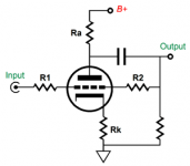
Is there a way to make a decent MOSFET version of an 'anode follower' using an enhancement mode MOSFET? (see attached image for vacuum tube anode follower example schematic)
Or...
I could make a 'solid state anode follower' out of a DN2535... No sweat. Just like working with a super-tube -- but no heater supply needed (sweet). Use 2:1 ratio for the two feedback resistors (series R input to gate and shunt R drain to gate).
What do you think? I'm sure somebody's tried that. What would be the downsides? Primitive, wasteful and poor performance compared to a good opamp? Or actually won't work in practice?
--
@jan.didden @Rick PA Stadel and everyone else who's responded
Yes, thank you very much for the insights.
1) I have a handful of DN2540 in TO-220 package. Biasing the source follower MOSFET is not a problem ('quiet bias' voltage divider from B+ to ground). What are the reasons to not use an IRF510 as the source follower with DN2535 (TO-92 package) as the CCS?
Biasing the CCS is the problem. A depletion mode MOSFET would certainly be easier to work with -- although it would require measuring/matching, or fitting out with a trimpot to dial in the Ids.
An LM217 (TO-92 pkg) would be a piece of cake to use. Rset = 1.25/Ids. The downside is that these voltage regulator ICs get inductive with rising frequency, so as a CCS their impedance falls with frequency with the audio band. According to some Walt Jung articles I've read, the LM317 as a CCS presents about a 1Mohm load below 5kHz, but begins to fall above that, falling to 100k ohms at 10kHz. Still, that's good enough to qualify as a truly constant current source in this application. It should be 'good enough'. Right?
2) It makes sense that the voltage divider resistors and gate load resistor would need to be made much smaller value. 360k and 390k maybe? (I guess I'm showing my high impedance/vacuum tube background.)
3)I could certainly massage values to set the source (output) at 1/2 B+.
4) Yes, it would be nice to have 6dB of gain, actually. Not required, but it would put the gain structure of my setup in a better place. Wouldn't an opamp like OPA2134 be the easiest (and 'best') way to accomplish this, using a 2:1 ratio for the feedback loop resistor values? That would be squeaky clean and everything. But then I'd have to go buy the opamps, and I was thinking I'd use up a couple of IRF510s for this.
I wonder...
Is there a way to make a decent MOSFET version of an 'anode follower' using an enhancement mode MOSFET? (see attached image for vacuum tube anode follower example schematic)
Or...
I could make a 'solid state anode follower' out of a DN2535... No sweat. Just like working with a super-tube -- but no heater supply needed (sweet). Use 2:1 ratio for the two feedback resistors (series R input to gate and shunt R drain to gate).
What do you think? I'm sure somebody's tried that. What would be the downsides? Primitive, wasteful and poor performance compared to a good opamp? Or actually won't work in practice?
--
Attachments
Last edited:
As mentioned before, R2, R3, R7 are rather large, not recommended. They could easily be 10x smaller for less noise and other parasitics.
As long as there is a signal source connected, large gate bias resistors only cause some deep subsonic noise. Above the corner frequency with the input DC blocking capacitor, the signal source basically shorts the noise of the resistors. In fact higher resistors will inject less noise current and lead to slightly less noise at frequencies above the corner frequency with the input DC blocking capacitor.
The large values do make the circuit unnecessarily sensitive to PCB leakage currents. That's mainly an issue when you want the circuit to work properly when the PCB is not perfectly clean (has flux residues for example) and is slightly damp. In my experience, PCB leakage currents are usually in the picoampere range for a clean and dry PCB at room temperature.
- Status
- This old topic is closed. If you want to reopen this topic, contact a moderator using the "Report Post" button.
- Home
- Source & Line
- Analog Line Level
- Viable Circuit? (Simple Source Follower using IRF510)