Thanks for the reply. I'm starting to see this as the best option as well. Ideally for the lowest distortion I would want to supply the op-amp with +/- 18V. As the board I am designing is using SMD components are you aware of any ICs which could take my 24V DC supply and create the +/-18V rails for the op-amps?Your life would be SO much easier if you just built a dual (+/-12 Volt) power supply. You have 10
opamps that have a quiescent load of less than 4mA each so a trivial 100 mA supply would deliver
2 times what you need.
The single supply version WILL have a turn on thump as all those caps get charged up so you will
need to add power on mute just to avoid the thump. You REALLY can't have that into the tweeter.
Someone mentioned resistors and caps in series. That is certainly easier than finding exact 2:1
component values to achieve Butterworth response. If you use surface mount it will cost almost
no PC Board space. Just remember caps in series don't add, they divide by 2.
I have done virtual grounds when absolutely necessary (in my car 30 years ago) but under
protest as the added parts are MORE than a dual supply. If I was doing opamps in the
car today I'd add a DC-DC converter to get the negative supply.
That solution could work for you too. If you're worried about switching noise use a +/- 15 volt
supply with linear +/-12 regulators to clean it up. I know with certainty that this approach works
well as I'm using an 8 Volt switcher with a 5 Volt regulator to supply my 5.1 optical DAC on the TV.
The improvement was well over 10dB.
DigiKey has +/- 15 Volt DC-DC converters less than $15.
G²
I imagine I could create the following: http://www.ti.com/tool/PMP10088 and use a step up converter to achieve the desired +/-18V
Are the 2xLM4562 you have used effectively the circuit shown in figure 2 here:Project 43 - Simple DC Adapter Power Supply ? Do you know if this would be sufficient for the number of op-amps I'm looking to drive?I've used both methods as shown in post #4 but the last one I did used a supply from a Silicon Chip design. Replaced a 317/337 supply that ran from a AC plug pack which resulted in a bit of noise in the pre amp. The pre is now quiet and runs from 12-24VDC plug packs.
The upper section runs the pre amp with 2xLM4562 and the lower section supplies 5V to relays and LEDs. I used 35V caps for the 220uF and 100uF.
It may look odd as it only has a 100uF cap to the -ve rail output and none to the +ve rail output but that's what the SC circuit showed. It's required to keep noise out from the plug pack so it doesn't get into the audio path. One other thing is to never run a device from the rails to the SG 0 virtual ground.... run across the rails such as shown for the 5V supply.
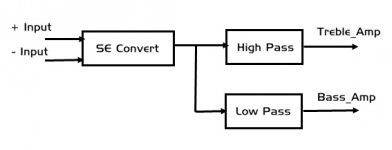
I was using them in series as it makes matching the resistors/capacitors easier. The crossover is designed for differential audio signals coming from a RN-52 BT audio module. Each of the high/low lines are fed to their own TPA3116D2 Amplifier.
So, the input to your crossover is a balanced (differential) signal from a bluetooth module.
I just know you're going to hate me for this but...
I would be concerned with phase issues and gain mismatches between the separate filters used on the hot and cold differential signals.
It seems to me it would make more sense to convert to a single ended signal, or if there is a low risk of common mode noise, to simply ignore one phase of the differential signals. Especially considering that TPA3116 chips use single ended inputs, this would cut your design complexity right in half as you would only need one high pass and one low pass filter for each channel.
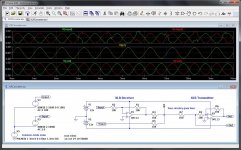
The first thumbnail is a simplified flow chart. The second shows a simple XLR (balanced) Receiver and Transmitter. You would most likely only need the receiver part.
In the spice screenshot, the top graph shows a differential input with considerable common mode noise, the middle graph shows how it's all cleaned up by the XLR Receiver, the bottom graph shows a nice clean differential output.
Attachments
Last edited:
Are the 2xLM4562 you have used effectively the circuit shown in figure 2 here:Project 43 - Simple DC Adapter Power Supply ? Do you know if this would be sufficient for the number of op-amps I'm looking to drive?
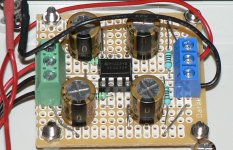
The 2xLM4562 are on the pre amp board only. My P43 supplies are built with a single TL082 or NE5532 (see example in pic). Rod said in the article that it's suitable for higher level stuff like crossovers and his active crossovers have heaps of op amps but someone with more knowledge on current requirements may chime in. Whether the current is dependant on the DC wall wart output or is restricted or not by this circuit?
There's an alternative to using a DC supply if you want to use a wall wart (plug pack). An AC wall wart can supply split rail DC using 317/337 or 78xx/79xx if you read the ESP P05 articles. P05-Mini
Attachments
Last edited:
Thanks for the reply. I'm starting to see this as the best option as well. Ideally for the lowest distortion I would want to supply the op-amp with +/- 18V. As the board I am designing is using SMD components are you aware of any ICs which could take my 24V DC supply and create the +/-18V rails for the op-amps?
I imagine I could create the following: http://www.ti.com/tool/PMP10088 and use a step up converter to achieve the desired +/-18V
A SilentSwitcher makes +/15 from a 5V Powerbank or USB charger. And extremely low noise too.
Jan
According to the datasheet the TPA3116D2 can use differential inputs. The receiving end of the amp takes R-, R+, L-, L+So, the input to your crossover is a balanced (differential) signal from a bluetooth module.
I just know you're going to hate me for this but...
I would be concerned with phase issues and gain mismatches between the separate filters used on the hot and cold differential signals.
It seems to me it would make more sense to convert to a single ended signal, or if there is a low risk of common mode noise, to simply ignore one phase of the differential signals. Especially considering that TPA3116 chips use single ended inputs, this would cut your design complexity right in half as you would only need one high pass and one low pass filter for each channel.
The first thumbnail is a simplified flow chart. The second shows a simple XLR (balanced) Receiver and Transmitter. You would most likely only need the receiver part.
In the spice screenshot, the top graph shows a differential input with considerable common mode noise, the middle graph shows how it's all cleaned up by the XLR Receiver, the bottom graph shows a nice clean differential output.
I would have hoped with the circuitry being identical there shouldn't be issues with phase shifts and differences in gain providing resistors are properly matched.
I will look into it further though.
Looks really cool but I'm making my own board which has lithium ion charging, amplifiers, active crossover, and BT module all in one. This would cause me to have a second external board.A SilentSwitcher makes +/15 from a 5V Powerbank or USB charger. And extremely low noise too.
Jan
According to the datasheet the TPA3116D2 can use differential inputs. The receiving end of the amp takes R-, R+, L-, L+
I would have hoped with the circuitry being identical there shouldn't be issues with phase shifts and differences in gain providing resistors are properly matched.
I will look into it further though.
But, there is also the matter of unnecessary complexity. Why build 4 sets of filters when you only need two?
In a project where (from what I gather) I'm building a bi-amped bluetooth system that will most likely be all in one box, running from a single power supply, I would bypass the differential signals entirely since common mode noise is very unlikely in that environment. I would grab one side of the differential outputs on the bluetooth module, use RCA jacks for any additional inputs and build the crossover and amp as a single ended device.
Now, if we were talking about separate devices, located some distance apart and interconnected by cabling, I might see more value in differential signalling, for it's noise rejection.
In any case, I was just looking over your schematic and old school me noticed a lot of duplicated effort and thought I should mention it.
Best of luck with your project...
- Status
- This old topic is closed. If you want to reopen this topic, contact a moderator using the "Report Post" button.
- Home
- Source & Line
- Analog Line Level
- Op-Amp DC power supply