I purchased several LME49713 op amps quite a way back and never did much with them except produce a simple headphone amp that worked well. It was P2P and I didn't have much issues.
Fastforward several years and I have finally decided to replace my Aunt Corey buffer that has done fine service for over 25 years. I started laying out what this circuit will look like and even briefly read up on the LM3886 thread for tomchr's recommendations for layout.
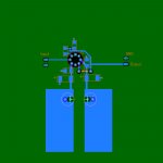
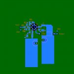
Where I have doubts is in the layout of the trace for feedback. I have followed recommendations in the datasheet for placement of feedback resistors and decoupling caps. I have opted for a 2 layer board for simplicity, with ground (green) being the lower layer, and traces for power rails and signals on the upper plane (blue).
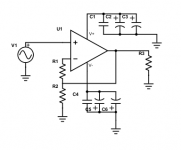
I've attached a rough schematic and a rough layout of what I think will work, but this is my first effort and trying a clean layout that will give good performance. Does anyone have 2 cents to share with me on how I've approached the layout? The TO-99 layout is a bit challenging so far.
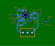
Pin 2 is inverting
Pin 3 non-inverting
Pin 4 V-
Pin 6 Output
Pin 7 V+
Additional comments(9/3/19):
Square pad is pin 1
R3 is actually Rload
J1 is a jumper wire that jumps the output signal over the positive power rail at 90 degrees to each other
SMD devices closest to pin 2 is the feedback resistor network
Intended voltage gain is intended to be around 3db for stability
Fastforward several years and I have finally decided to replace my Aunt Corey buffer that has done fine service for over 25 years. I started laying out what this circuit will look like and even briefly read up on the LM3886 thread for tomchr's recommendations for layout.
Where I have doubts is in the layout of the trace for feedback. I have followed recommendations in the datasheet for placement of feedback resistors and decoupling caps. I have opted for a 2 layer board for simplicity, with ground (green) being the lower layer, and traces for power rails and signals on the upper plane (blue).
I've attached a rough schematic and a rough layout of what I think will work, but this is my first effort and trying a clean layout that will give good performance. Does anyone have 2 cents to share with me on how I've approached the layout? The TO-99 layout is a bit challenging so far.
Pin 2 is inverting
Pin 3 non-inverting
Pin 4 V-
Pin 6 Output
Pin 7 V+
Additional comments(9/3/19):
Square pad is pin 1
R3 is actually Rload
J1 is a jumper wire that jumps the output signal over the positive power rail at 90 degrees to each other
SMD devices closest to pin 2 is the feedback resistor network
Intended voltage gain is intended to be around 3db for stability
Attachments
Last edited:
The schematic is wrong. The nfb network should have a resistor from the output to the inverting input, and another resistor from the inverting input to ground. There should be a resistor from the positive input to ground. Also, there's no need for a resistor from the output to ground.
Last edited:
I purchased several LME49713 op amps quite a way back ears and I have <snip>
Are you familiar with current feedback amplifiers? They're a little different from the
much more common Voltage feedback amplifiers. You're much more limited on the feedback
resistor since that value also sets the response of the amp. With a 1900 V/uS amplifier you
do not want to connect the inputs and output directly to the amplifier as the cable capacitance
is possible to make a fine oscillator. Add a series resistor to the output and another to the
input to decouple stray capacitance. On the output side I'd use a value between 10 and
100 ohms. If it needs to deliver more current you can go below 10 but I think 0 will give
you issues. Input side somewhat larger.
Rayma is correct about the feedback.
Post your altered schematic before you make the PCB. We might save you
a little time.
I would definitely be checking it out with a scope to be sure about oscillations.
G²
Thanks for all the great responses. I'm at work so I can't go into depth here, but I made an addendum in my original post.
Rayma, the datasheet mentions that the output node is sensitive, so it recommends placement of feedback resistor closest to the input nodes. R3 is the load (my amplifier). Notice at the output that I have a jumper wire over the positive power rail and that it feeds back to the resistor network by the #2 pin. I plan on using a pair of Susumu surface mount resistors.
Again, I appreciate all the input and opinions!
(Ok, see the error now in my routing! I appreciate it. Can't believe I screwed that one up)
Last edited:
Noted that I forgot the resistor at the input that runs to ground.
stratus46 - Yes, I was in contact for a very short time with Mark Brasfield when he worked on the LME project at NatSemi. He pointed out the same things that you did, but in his case, he said it should be stable with a feedback value of 1k2 ohms. I'm a little leery of doing that and I will pick a slightly higher value, like you mentioned.
I made my interconnects from Belden wire and planned to calculate the total capacitance, but added insurance with resistors at input and output is what I prefer. Several years ago I worked with these devices quite a bit and they sometimes worked and sometimes would go into oscillation. After scouring the net, I realized I likely had issues with stray capacitance. It pays to do the homework and this is why I wanted extra eyes on this before I sink some money into boards that end up in the trash bin.
I just want to be sure I don't lose signal integrity by jumping the output over the positive rail. But from what I've read on some of the posts here, I think I should be good. I just got stuck trying to decide on a layout that is better.
Side story - Mark sold me some AD811 chips that he had sitting on his bench and told me that he based the 49713 on the AD chip because he really liked the sound he heard when using them.
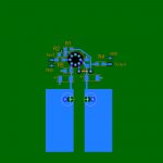
Both pins 1 and 8 are said to be NC. If they really are, then you can use pin 1 as a tie point,
to drastically shorten the trace from the output to the feedback resistor. That is, directly connect
pins 1 and 6 with a short trace underneath the IC.
Then the output resistor R4 can take the place of the jumper, and the cap on pin 7 can move upward
for a shorter connection. Also, vias to the ground plane should have thermal relief.
Last edited:
Rayma, got it. I'll work on your recommendations.
I always solder vias on my boards. Actually I use pads, so there's no solder mask on them.
But few do that, so the thermal reliefs aren't needed here.
If it turns out pins 1 and/or 8 do have an internal connection and are not true NC, you can always
just cut off that lead before mounting. The data sheet says nothing else, though.
Last edited:
<snip>
Side story - Mark sold me some AD811 chips that he had sitting on his bench and told me that he based the
49713 on the AD chip because he really liked the sound he heard when using them.
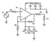
I've used many AD811s in High Def video systems. Your current schematic is pretty much what I would expect.
I would add 1 more resistor from R5 to ground. If for some reason the input signal V1 is disconnected it will
maintain a ground reference and not go slamming a rail or possibly oscillate.
I wouldn't get too worried about the track length. The AD811 is even faster and I never had one misbehave and
AFAIK not one has ever failed in over 25 years out of nearly 1000 pieces.
My guess is the sound Mark liked is because of the speed and also the output current capacity.
G²
Further changes based on the input I've received. All very good points!
My only one concern in comparing my layout with tomchr's LM3886 layout is that he has signal grounds kept away from the power rail grounds and he noted that it makes a difference.
So if there is no penalty in longer signal traces, I want to have the output closer to pin 8 to get it away from the positive rail grounds and more in a quieter zone of the pcb.
The long term goal is to learn from this one and design other boards in similar layouts and sizes so I can swap them out easily. A buddy of mine hangouts out with folks from the Houston Audio Society and he told me he hears lots of positives about the AD823a.
stratus46 - I added R6 to ground. Is that placed correctly or the other side of R5? Good to know about the AD811. When Mark sent me those, they worked pretty easily. The LMEs seem to be much more fiddly. He recommended running them as inverted and boy I had to read up on that because of the low impedance on pin 2. I got it to work but sometimes had issues with swinging DC offset.
rayma - yeah, I've heard of using pads instead of the vias and then filling the hole with solder, so I'll give that a go. I'm flexible, as you maybe can tell. I even switched R4 to through-hole so I could get more area for the power rail.
I still have some cleanup on the board, so apologies for the rough appearance. I just want to be sure I get all the important things done right before I order the board.
Attachments
Last edited:
The two lands don't really do anything, so delete them and just move the electrolytics closer in.
Flip the small and medium positive bypass caps upward so they are out of the way, and then
the + electrolytic trace can be more direct.
Move R1 rightward so its right pad is directly over pin #1. Connect R6 instead to the left end of R5,
and move R5 in closer to the IC.
When using pads in place of vias, the hole can be larger, have better plating, and be more reliable,
as well as be soldered. Where is the connector for the power supply?
Last edited:
Rayma, ok. I thought the idea of large lands was to have lower impedance on the power rails.
But I guess this doesn't matter as much with a preamp.
A direct, short trace will work as well or better here. Also, most of the hf current will go through
the two ceramic caps.
If you're really after the best possible layout you'd also want to consider common-mode currents. They'll flow between the 'GND' terminals on your PCB depending on what you have connected as source and load equipment.
If your load is a pair of headphones then you only need to consider CM currents flowing between your power supply (if mains fed) and your source equipment (also if its mains powered). If either your source or this preamp (or both) is/are battery powered then you won't have any worries.
Assuming you do have a mains fed source and your preamp is the same then you'll want to route currents between the two GND pins so they don't induce voltage drops between other GND nodes.
Here's the latest version. Rayma, I hope I read you right. If not, I know you will guide me. I feel like I'm close. I added references to the caps now and included a terminal block for power rails and ground.
abraxalito,it will be my DAC, powered via the mains, and the preamp powered by the mains, going to my amp, powered by mains. No batteries. Not sure how to route currents between two ground pins.
BTW, the headphone amp I wired up on protoboard years ago was powered by two 9 volt batteries. I was very impressed by the sound from those two op amps and basically got a "told you so" from Mark when he asked for feedback.
Attachments
- Status
- This old topic is closed. If you want to reopen this topic, contact a moderator using the "Report Post" button.
- Home
- Source & Line
- Analog Line Level
- Need an opinion on layout of LME49713 preamp