it will be my DAC, powered via the mains, and the preamp powered by the mains, going to my amp, powered by mains. No batteries. Not sure how to route currents between two ground pins.
The simplest solution is to move either the input or the output pins so they're adjacent to one another. Then there's just a short path from input GND to output GND and no noise currents to speak of will flow through your groundfill.
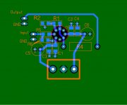
I added references to the caps now and included a terminal block for power rails and ground.
I would flip the lower ends of C2 and C4 upward (similar to the negative supply caps).
Then you will have room to move C6 and the vertical positive bus leftward, closer to the IC.
Also move R6 left a bit so its left pad is below the IC output pin.
Last edited:
abraxalito,
Ok, no longer confused. This was something I brought up earlier, about moving the output to a "quieter" zone of the ground because I had it located close to the positive rail. tomchr commented that placement of the LM3886 output made a difference when he kept the output away from the rails.
Ok, no longer confused. This was something I brought up earlier, about moving the output to a "quieter" zone of the ground because I had it located close to the positive rail. tomchr commented that placement of the LM3886 output made a difference when he kept the output away from the rails.
The caps I plan to use are .1 uF X7R, around 20 uF tantalum, and 220 uF electrolytic. Reasonable?
With such a high bandwidth op amp, I'd use a 0.01uF ceramic, 0.1uF ceramic, and an electrolytic.
Ok, just caught the comments regarding cap choices. A lesson in "popular wisdom says"
not fitting all situations. I'll make those changes.
Also should verify with TI that pin #1 is a true NC. Sometimes a NC is not really a NC.
The data sheet is silent.
This was something I brought up earlier, about moving the output to a "quieter" zone of the ground because I had it located close to the positive rail. tomchr commented that placement of the LM3886 output made a difference when he kept the output away from the rails.
I suspect that issue was a slightly different one - with a classAB output stage the positive and negative rails are very noisy with half-wave rectified versions of the output signal imposed on them. The decoupling capacitors used on power pins are also coupling capacitors to the groundfill. The point where those caps attach to the GND becomes 'noisy' too so you want to keep away anything remotely sensitive.
In this instance the 'noise' is coming in from outside, from your external equipment. But otherwise the principles to apply are exactly the same - arrange for the 'noise' to be contained somehow.
The pins are listed as "NC" on the datasheet and TI's standard practice with pins labeled NC means that there is no internal connection to these pins. So, it seems safe to use these pins as a way to route traces through the package. I can't think of a use for these pins either - there are usually no offset adjustment or compensation features on CFB amps, so I'm not sure what else these pins would attach to.
I'm not TI however, and this is not authoritative, but TI does seem to have standards for its documentation, and if a pin has internal connections, they seem to tell you about it and not just say "NC". If you happen to blow one up, you could lift the lid and find out!
I'm not TI however, and this is not authoritative, but TI does seem to have standards for its documentation, and if a pin has internal connections, they seem to tell you about it and not just say "NC". If you happen to blow one up, you could lift the lid and find out!
Then I'd assume this is ok and go ahead and complete the layout. Bear in mind that you always want
to order a minimal number of boards first to prove the design anyway. Osh Park would be perfect
for this. Three copies and shipping for only $5 per square inch of the layout. Excellent quality boards.
to order a minimal number of boards first to prove the design anyway. Osh Park would be perfect
for this. Three copies and shipping for only $5 per square inch of the layout. Excellent quality boards.
Last edited:
Monte,
Thanks for the input. My only concern is that this was a Nat Semi design and TI decided fairly quickly to kill production after the acquisition. Not sure if TI had interest in reviewing the datasheets.
Rayma, yeah, I had the same idea. I didn't want to sink good money into several boards, just a small number.
Revisions coming up on the latest recommendations.
I didn't want to sink good money into several boards, just a small number.
Also I would socket the first board.
Three rules to follow.
Keep the loop area as small as possible. - Place return path under the input path is a good way of doing this.
Connect the reference points together where the voltages are important. - Connect the input and output grounds together.
Dont mix signals in the ground plane.
Keep the loop area as small as possible. - Place return path under the input path is a good way of doing this.
Connect the reference points together where the voltages are important. - Connect the input and output grounds together.
Dont mix signals in the ground plane.
Latest and greatest. Yep, socket would be much easier here.
Don't run the output all over the place past the input/feedback circuitry, if you want a stable circuit.
Jan
- Status
- This old topic is closed. If you want to reopen this topic, contact a moderator using the "Report Post" button.
- Home
- Source & Line
- Analog Line Level
- Need an opinion on layout of LME49713 preamp