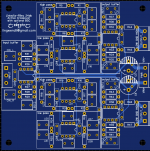
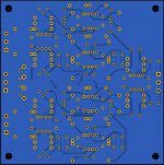
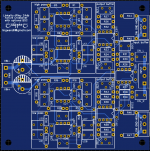
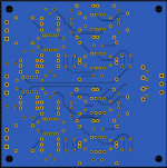
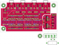
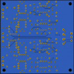
So, I haven't touched a solder iron for any audio projects in months, and wanted to put together a PCB design to hold me over. This is more-or-less the same as the ESP p09 crossover, but with the option of building the buffer opamp at the input as a shelving low-pass filter for baffle step correction. I oringinally decided on a ground plane, now I'm not so sure. I'm currently torn on which version to keep on working with. I modified the ground plane to have a central ground rail with a semi-star arrangement for the connections.
Anybody have an opinion? I feel like the ground plane idea is likely best, but some are adamant about using a star arrangement with such things. I have the ground plane connected only at the power GND terminal on the star/rail version, with it throughout the board as a sheild only. I can easily delete the sheild and use only the star/rail too.
Yes, I will be posting design files once done")
Anybody have an opinion? I feel like the ground plane idea is likely best, but some are adamant about using a star arrangement with such things. I have the ground plane connected only at the power GND terminal on the star/rail version, with it throughout the board as a sheild only. I can easily delete the sheild and use only the star/rail too.
Yes, I will be posting design files once done
Attachments
Last edited:
Here are my thoughts for what it's worth. From an EMC perspective ground planes are nearly always better. With a good PCB layout the ground current will still flow where you want; without any need for star connections or separated grounds.
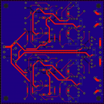
However on both version of your PCBs if you form a ground loop, as the input and outputs are on opposite sides of the PCB, then that ground loop current will be flowing through the ground nodes of the filter circuits.
My understanding is that it is better to have the inputs and output grounds next to each other, so swap the locations of power and input, so any ground loop currents are away from the filter circuit. Unless you then connect the power supply to earth as well, guess you would want them all at one end of the PCB then.
Last edited:
I'm in favor of using ground planes whenever there is no good reason not to do so. They help to keep loop areas small, reducing pick-up of any RF fields that may be around.
(If you would have included a power supply, I would advise you to keep the return paths of the smoothing capacitors separate from the ground plane, but it looks like the electrolytics are just for decoupling.)
(If you would have included a power supply, I would advise you to keep the return paths of the smoothing capacitors separate from the ground plane, but it looks like the electrolytics are just for decoupling.)
Hmmm.
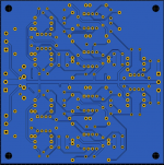
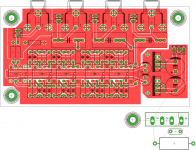
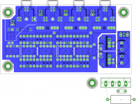
So, following what you're saying- I'll swap the input buffer circuitry to the right side of the board, and then that'll keep the power stuff all on the opposite end from the input/output connections. I'll just need to bring the input traces back the other way, but it makes much more sense to keep it all signal on the one side, power on the other. Thanks!
So, following what you're saying- I'll swap the input buffer circuitry to the right side of the board, and then that'll keep the power stuff all on the opposite end from the input/output connections. I'll just need to bring the input traces back the other way, but it makes much more sense to keep it all signal on the one side, power on the other. Thanks!
Rules i set to myself:
1. Always star ground.
2. Put all i/o connectors in same place
3. Never separate power rails, put power supply closest to the heaviest load.
4. Remove the star ground and put solid plane. Cut planes if you have to. If everything is right, no cuts needed.
5. Filter everything going in and out. Ferrite/ceramic caps/CM chokes/T-filters on PS, T-filters/CM chokes on analog. CM are not always necessary/good.
These analog low-power devices might benefit from heavy local bypassing (extremely low esr solid caps + np0/pps + series R to main regulator).
Print the pcb, take a pen and draw supply and return circles/currents for PS and analog signals.
They should not intersect kinda strict, but well...
1. Always star ground.
2. Put all i/o connectors in same place
3. Never separate power rails, put power supply closest to the heaviest load.
4. Remove the star ground and put solid plane. Cut planes if you have to. If everything is right, no cuts needed.
5. Filter everything going in and out. Ferrite/ceramic caps/CM chokes/T-filters on PS, T-filters/CM chokes on analog. CM are not always necessary/good.
These analog low-power devices might benefit from heavy local bypassing (extremely low esr solid caps + np0/pps + series R to main regulator).
Print the pcb, take a pen and draw supply and return circles/currents for PS and analog signals.
They should not intersect
kinda strict, but well...
Last edited:
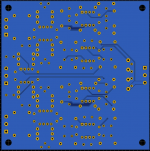
One fact its worth knowing about groundplanes in standard 1oz copper pcb is the resistance per-square is about 0.5milliohm, ie 0.0005 ohms. 10mA flowing between two arbitrary places on a large ground plane is going generate something in the order of 5 or 10µV. If the signal level is about 1V, that's -100dB down. Something like an active crossover or line preamp isn't going to be troubled by this. A microphone or phono preamp is a different matter.
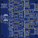
Make the power traces wide to lower stray inductance and resistance (and much easier to follow them for testing/debugging) I find with a 2-layer board they have to weave between front and back a bit to avoid breaking the ground plane up to much. The most important thing is that the trace between a supply pin and its decoupling capacitor is short and wide, especially with high bandwidth opamps, since the impedance at 10 to 100MHz is all important for its function.
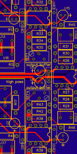
I just redid some of the power traces, and upped them to 1mm width, which should be nice for these opamps (likely OPA2132PA since I have planty on hand) and should be getting close to done.
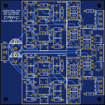
Any suggestions on opamp bypassing? Since I don't plan to use cranky opamps here I went with the oft-recommended (by datasheets at least) cap from each rail to ground. Should I put in the option to put one from rail-to-rail at each opamp as well?
Any suggestions on opamp bypassing? Since I don't plan to use cranky opamps here I went with the oft-recommended (by datasheets at least) cap from each rail to ground. Should I put in the option to put one from rail-to-rail at each opamp as well?
Last edited:
That be for DC. At higher frequencies than DC you want return paths near signal traces as well as better decoupling of opamps.One fact its worth knowing about groundplanes in standard 1oz copper pcb is the resistance per-square is about 0.5milliohm, ie 0.0005 ohms. 10mA flowing between two arbitrary places on a large ground plane is going generate something in the order of 5 or 10µV. If the signal level is about 1V, that's -100dB down. Something like an active crossover or line preamp isn't going to be troubled by this. A microphone or phono preamp is a different matter.
Allthough this is low frequency there might be high frequencies near by. Ground plane increases the imunity to HF entering the signal traces.
Common misconception that circuits only work in the frequency range you want.
If you stick a Wi-Fi router next to your PCB, the PCB traces could unintentionally turn into nice little antennas/transmission lines. Previous EMC testing has shown me any interference above 2GHz easily becomes an issue even on the best PCB layout.
With bypassing requirements; power rail to ground next to each opamp supply pin is good, use 100nF ceramic and 10uF electrolytic or similar. Having capacitors (again 100nF and 10uF for example) every couple of inches between positive and negative supply rails can help. For example you could fit them in next to CB10, CB11, CB13.
Any suggestions on quality, affordable rail caps in the 10~47uF range for the local bypassing, from digikey? 2.5mm or 5mm lead spacing? I don't do lower volatage often, so I'm having a hard time choosing something suitable here. I'm thinking 16 or 25 volt is plenty, as the intended application will likely call for 12 or 15 volt rails.
Do these 25 volt, 47uF guys look good? Nice long life and decent ratings-
ULD1E470MDD1TD Nichicon | Capacitors | DigiKey
Do these 25 volt, 47uF guys look good? Nice long life and decent ratings-
ULD1E470MDD1TD Nichicon | Capacitors | DigiKey
Spec wise those Nichicons look good. Panasonic FC parts are always a safe bet, supposed to sound good as well...
Example
EEU-FC1H220H Panasonic Electronic Components | Capacitors | DigiKey
Example
EEU-FC1H220H Panasonic Electronic Components | Capacitors | DigiKey
- Status
- This old topic is closed. If you want to reopen this topic, contact a moderator using the "Report Post" button.
- Home
- Source & Line
- Analog Line Level
- Crossover PCB in progress, ground plane or star/rail?