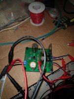
I decided to do this so that I can have PCB that will drive various OPS for experimentation. The 4 transistors were each under $1 bought in quantity. Many days of curve tracing to create matched pairs.
All of the resistors, terminal blocks and PCB together probably cost more than the semiconductors.
If I burn up this board while experimenting, I will not be throwing away a bunch of money. On the other hand, making such an experimenter board from PL JFETs and MOSFETs would be relatively expensive.
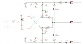
+ / - 35V rails. 3mV DC output offset. 2.2mA bias front end. 10mA bias second stage.
Gain slightly under 10x
Output impedance 55-ish ohms.
Better than 60v p-p before clipping.
Bandwidth is insane. -3dB 14.3 MHz with a peak 10-ish MHz. Phase is quite wonky out in the MHz space.
Good enough to use as a driver for various OPS experiments.
Front end devices are 2SA970BL/2SC2240BL
Output devices are KSA1381E/KSC3503E
Feedback resistors ended being 1k after some experimentation. The schematic will be changed to reflect 1k feedback resistors.
All of the resistors, terminal blocks and PCB together probably cost more than the semiconductors.
If I burn up this board while experimenting, I will not be throwing away a bunch of money. On the other hand, making such an experimenter board from PL JFETs and MOSFETs would be relatively expensive.
+ / - 35V rails. 3mV DC output offset. 2.2mA bias front end. 10mA bias second stage.
Gain slightly under 10x
Output impedance 55-ish ohms.
Better than 60v p-p before clipping.
Bandwidth is insane. -3dB 14.3 MHz with a peak 10-ish MHz. Phase is quite wonky out in the MHz space.
Good enough to use as a driver for various OPS experiments.
Front end devices are 2SA970BL/2SC2240BL
Output devices are KSA1381E/KSC3503E
Feedback resistors ended being 1k after some experimentation. The schematic will be changed to reflect 1k feedback resistors.
Attachments
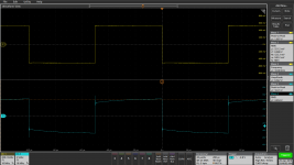
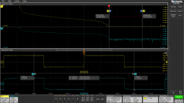
Here is a scope shot of a 10kHz square wave. Not good. Yellow trace is input and blue trace is output.
At the moment, there are no compensation components installed. C4 in the schematic is not yet installed.
What value components and where to be installed to make a good looking square wave. This is my first from scratch build so its a bit a new venture.
At the moment, there are no compensation components installed. C4 in the schematic is not yet installed.
What value components and where to be installed to make a good looking square wave. This is my first from scratch build so its a bit a new venture.
Attachments
Bandwidth is high as there is no miller compensation and the output transistors have 150MHz GBP. Hopefully its not a VHF oscillator when loaded capacitively
The component values don't agree with the values you quote, the bias at 35V ought to be more like 40mA in the second stage with 10 ohm emitter resistors. And the gain should be pretty close to x23 with those feedback values as there should be plenty of open loop gain.
The biasing will vary with supply voltage significantly - those OFF1 and OFF2 resistors need to be set for the voltage - constant current circuits are more flexible here.
If the second stage bias is 10mA as you say, then the maximum signal swing is limited by the heavy load presented by the two 2k2 feedback resistors in parallel.
If the bias is more like 40mA then that won't be a limitation.
Here is a scope shot of a 10kHz square wave. Not good. Yellow trace is input and blue trace is output.
At the moment, there are no compensation components installed. C4 in the schematic is not yet installed.
What value components and where to be installed to make a good looking square wave. This is my first from scratch build so its a bit a new venture.
Have you tried with a low amplitude sine input, that square wave will be overloading the input stage perhaps, I suspect the output is struggling to drive the feedback network.
There's definitely too much ringing on the output, that's a sign of near-instability. Try 22pF miller caps on the outputs.
Have you tried with a low amplitude sine input, that square wave will be overloading the input stage perhaps, I suspect the output is struggling to drive the feedback network.
There's definitely too much ringing on the output, that's a sign of near-instability. Try 22pF miller caps on the outputs.
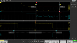
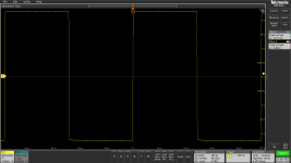
Sine waves look good. I dialed back the square wave to 100mV p-p input yielding 920 mV p-p output. No change in the shape of the square wave output.
I will begin adding capacitance from base to collector for the two output transistors. I will also try a series R-C zobel while I am at it.
There may be some oscillation happening. The sine waves are being visibly DC offset modulated where the entire sine wave is moving up and down at 4 Hz -ish. The amplitudes are not changing.
I will see if I can get a spectrum view of the output and input.
Bandwidth is high as there is no miller compensation and the output transistors have 150MHz GBP. Hopefully its not a VHF oscillator when loaded capacitively
The component values don't agree with the values you quote, the bias at 35V ought to be more like 40mA in the second stage with 10 ohm emitter resistors. And the gain should be pretty close to x23 with those feedback values as there should be plenty of open loop gain.
The biasing will vary with supply voltage significantly - those OFF1 and OFF2 resistors need to be set for the voltage - constant current circuits are more flexible here.
If the second stage bias is 10mA as you say, then the maximum signal swing is limited by the heavy load presented by the two 2k2 feedback resistors in parallel.
If the bias is more like 40mA then that won't be a limitation.
The feedback resistors are 1k. With 2.2k feedback resistors, the output stage bias is 20 mA -ish. These both agree with the sim attached.
From a sine wave standpoint, the output swing is 63v p-p at 1kHz before onset of visible clipping.
Attachments
Last edited:
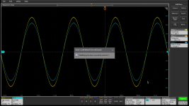
Yellow is the signal source feeding the preamp.
Successfully have Spectrum View running alongside of Waveform View. My guess here is that the signal generator I am using is passing the internal digital clock and the preamp is doing a good job of amplifying the clock bleed through along with all of the clock's overtones.
Time to see if I can find the analog sig gen.
Attachments
Success
Happy to report that the circuit is working. Installed 20pf compensation caps and a 68 pf input RF killing cap.
Once those were sorted out, I was able get a screen shot of a 10kHz square wave which is attached.
This is now complete as a prototype. There are a few tweaks for ease of build and debug. Need to add the comp caps to the schematic and board.
Attachments
Resurrected this circuit to drive a new power amp project.
Installed 2SC2240 and 2SA970 for front end. Installed BD139 and BD140 for output. Rails + / - 33V. Front end idle current ~2mA. Output stage current ~ 23mA.
Maximum sine wave voltage before clipping is 64.5 vp-p. Voltage gain is ~ 42. Output impedance is ~ 70 ohms.
Installed 2SC2240 and 2SA970 for front end. Installed BD139 and BD140 for output. Rails + / - 33V. Front end idle current ~2mA. Output stage current ~ 23mA.
Maximum sine wave voltage before clipping is 64.5 vp-p. Voltage gain is ~ 42. Output impedance is ~ 70 ohms.
Attachments
- Status
- This old topic is closed. If you want to reopen this topic, contact a moderator using the "Report Post" button.
- Home
- Source & Line
- Analog Line Level
- VSSA as preamp/driver