I'm working on a preamp design and like the look of the INA1650 for the balanced input. The datasheet advises a 10uF dc blocking cap on the inputs and then a proposed layout with those caps shown in a smd package. Until that point I was assuming those caps would be electrolytic (or i was thinking of a couple of 4.7uF PP in parallel)... Am I missing something, is there an SMD 10uF cap that would be suitable in this application - C0G/NP0 don't get any where near that value and I've never considered putting other types of ceramic in the signal path.
Attachments
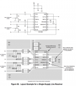
The datasheet advises a 10uF dc blocking cap on the inputs and then a proposed layout
with those caps shown in a smd package.
These types would be the normal industrial choices.
http://uk.farnell.com/multicomp/mcesl25v106m5x5-2/cap-alu-elec-10uf-25v-smd/dp/1870611
F951E106KBAAQ2 AVX | Mouser
I just wondered if there was a decent quality (for an audio signal) cap in this value
and package and as they show a non-polarised component
That diagram was more to give an idea of a layout, just not with any particular parts.
A nonpolar X7R smt ceramic type could indeed be used in some applications (high temp, etc.).
I guess so... I think I'll either go with a bigger electrolytic à la Douglas Self or use a couple of film caps.That diagram was more to give an idea of a layout, just not with any particular parts.
I guess so... I think I'll either go with a bigger electrolytic à la Douglas Self or use a couple of film caps.
Because the input impedance of the INA1650 is high, the high-pass corner frequency formed by the 10uF cap and the input resistors is very low, meaning minimal voltage appears across the 10uF caps at audio frequencies and they do not contribute significant distortion. Of course electrolytics are fine as well.
Yes, 10uF and 1M mean an LF corner frequency around 15mHz. That means that a 15Hz 1V signal will develop about 1mV across the cap. If the cap is more horrible and nonlinear than any cap could ever be it might develop 0.1mV of distortion i.e. -80dB. I don't think you have anything to worry about in real life.
I would not use an electrolytic, as leakage current might be an issue into a high impedance input. You could use a 0.1uF film cap and get a 1.5Hz rolloff.
I would not use an electrolytic, as leakage current might be an issue into a high impedance input. You could use a 0.1uF film cap and get a 1.5Hz rolloff.
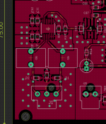
I finally got around to using the INA1652, schematic & layout attached. When I power up the output of the IC has an offset rising at a at a rate of 1mVDC every few seconds. I'm only using one channel so I've grounded the other one.
Having gone back to the datasheet I realised that with a dual supply the Vmid pins should be left floating so I cut them to disconnect them from ground... this has had no effect.
Any ideas what's going on here?
Having gone back to the datasheet I realised that with a dual supply the Vmid pins should be left floating so I cut them to disconnect them from ground... this has had no effect.
Any ideas what's going on here?
Attachments
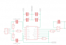
You appear to have no path for input DC bias currents, since DC0 does not connect to chassis ground. That tends not to work too well...
BTW, I'm not sure why the OPA1650 datasheet suggests 100k for R1/R2. They drop common-mode input impedance quite a bit. The IC itself has (250k + Rcom) = 1.25 Megohms, with these it drops to (250k + Rcom) || 50k ~= 48 kOhm. Still better than a run of the mill circuit (~10-20k, typ) but not by leaps and bounds. At the same time, differential input impedance remains fairly high at almost 170k. Left hand not knowing what the right one does or something.
Not sure how to fix this elegantly. I would probably lift R1/2 from (what ought to be) chassis ground and squeeze in an additional 1 Meg resistor to chassis ground for another T-type connection, while going from 100k to 22k resistors (or even 10k, dissipation permitting). That would get us (1.011 || 1.25) Megohm = 559 kOhm common-mode and ~42k differential mode.
Thanks for looking... I've just realised that J1 is incorrectly labelled it should be sig+, chassis, sig-. Nothing's in a chassis yet, the DC offset condition arises when I have all three inputs of J1 shorted to ground.
Thanks for the other advice, I'll look at the common-mode input impedance once I've got the circuit working as per the data sheet.
Thanks for the other advice, I'll look at the common-mode input impedance once I've got the circuit working as per the data sheet.
- Status
- This old topic is closed. If you want to reopen this topic, contact a moderator using the "Report Post" button.
- Home
- Source & Line
- Analog Line Level
- INA1650 DC Blocking