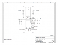
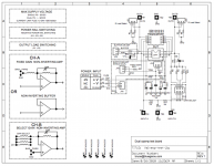
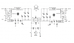
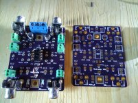
Test jig for dual opamps
I became tired of throwing together a dual pkg test jig that allows both non-inverting buffer and inverting amplifier.
So building up a test board design in the spirit of fivefish but simplified and dual amp dip8 package.
Ch A is dedicated buffer and ch B is inverting amp.
Take a look at schematic and let me know if issues.
The signal input-outputs will be on turrets for clip leads and scope probes etc.
Board will be at least 2.5"x2.5" for better stability on workbench when the valve module is plugged in.
-
Attachments
If you're using a non-inverting amplifier topology, there is an effect found with junction isolated JFET input stages that is worth considering. Basically, the input common mode signal voltage modulates a parasitic drain to substrate capacitor on each input FET, adding distortion that rises at 6dB/octave. These papers explain it in more detail:
http://www.analog.com/media/en/technical-documentation/application-notes/742022599AN232.pdf
http://www.ti.com/lit/an/slyt595/slyt595.pdf
These effects won't happen with an inverter, since the inverter topology results in no common mode signal voltage applied to the input stage, and thus no modulation of this parasitic nonlinear capacitance, so it doesn't tickle this form of distortion. However, most people who use JFETs do so for high impedance non-inverting stages, and thus encounter this problem.
There are other reasons for an amplifier to misbehave with common mode input signals, so in general, if you can use an inverter, your circuit will be much cleaner.
-
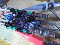
I was done with the dual opamp test board then remembered this issue with non-inverting. I want to analyze more on it so added an amp mode to the non-inv buffer channel. Then I also remembered this tube hybrid circuit is going to be used both in single and dual supply. So have added those switching shunts. Then I thought it would be nice to be able to analyze the op-amp itself prior to soldering. So I added test socket provision for SO8 and SOP8.
Its more complex now but worth it.
The documentation showing shunt positions is not finished, checking netlist now.
We'll see in a few weeks.
-
Attachments
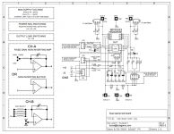
Found a hard error on JP6 and a design error on bias filter.
It was possible if operating dual supply, for a user to power up the minus supply and not positive.
If bias filter is tan or electrolytic then it could be damaged.
I made it 10uF 50v ceramic X5 ( I had a reel of them).
I also cleaned up power input and replaced fuzes with 1.0 ohm 1206 resistors.
The previous schematic had the minus fuze always in circuit. Now if operating single supply the minus(gnd) fuze is no longer in gnd supply.
The SOIC adapter strips probably could be eliminated by using TS-xxx-G-A headers on SO adapter. But I'm leaving them in.
-
Attachments
")
Sure no problem, the BOM will be shown on schematics next rev. I try to put everything on one sheet. Assy notes too.
Note: I did remove the header strips for SO8 socket. The Fb path was just too degraded using those ZIF sockets.
There is a Rev coming on both composite DIP8 board and test board. No errors just clean up text and shove around for better clearance.
-
Note: I did remove the header strips for SO8 socket. The Fb path was just too degraded using those ZIF sockets.
There is a Rev coming on both composite DIP8 board and test board. No errors just clean up text and shove around for better clearance.
-
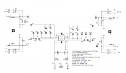
Sort of a status update: Now have layed out and ripped-up the test/eval motherboard several times. Just did not like the design.
Looked at sq pin headers for config, micro screw terminals, solderless breadboard and so on.
Now doing a layout with Keystone/mill-max pin receptacles.
Both channels are configurable as buffer, current mode buffer, inv amp, non-inv amp and differential amp.
Adding Numerk 1/4" jacks and/or RCA jacks.
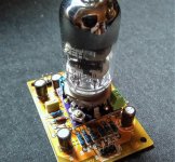
Here is a phono stage came in mail yesterday.
I removed the ne5532 and plugged in the module.
Untested still.
Pic.
Looked at sq pin headers for config, micro screw terminals, solderless breadboard and so on.
Now doing a layout with Keystone/mill-max pin receptacles.
Both channels are configurable as buffer, current mode buffer, inv amp, non-inv amp and differential amp.
Adding Numerk 1/4" jacks and/or RCA jacks.
Here is a phono stage came in mail yesterday.
I removed the ne5532 and plugged in the module.
Untested still.
Pic.
Attachments
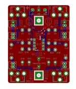
The test platform is taking much longer than expected.
Have finally settled on Keystone micro-jacks. They are very inexpensive in qty.
Pic and Bom.
-
Dropped the neutriks and a few other things. All done with drills, silk etc now just a few hours from sending to fab.
Added provision for AC coupling for TBD tests and added a terminal for hardwire to ext reactive loads.
I'll be happy to get this out of the way. Its important because I will be doing a new opamp/tube design with high bandwidth , no Miller effect so the board could see 10Mhz and up.
pic and schematic
-
Attachments
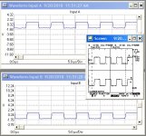
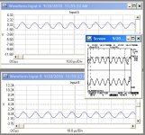
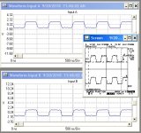
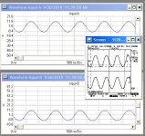
While waiting on the test platform thought I would look at the compensation requirements in more detail.
These plots are using a JJ 12AU7/ECC82 as the valve section. The opamp is still extended temperature OPA1612AQDRQ1. Earlier today did same run of tests with the EH 6922 but did not capture screens.
On the series resistors within comp circuit, these are unnecessay so they are jumped out with bus wire.
One of the project goals is to eliminate slurr and TIM. These plots are showing 100khz and 1Mhz operation, unity gain, both channels driven and no load resistor.
Onset of sine clipping is around 21.5 to 22.0 Vpp.
I have found that a single value comp capacitor ( 68pF ) will work on both the RF tubes and low frequency 12AU7. The 1k grid resistor also seem to be a good value.
The file names have test descriptions.
From my old Fluke 97 with Flukeview.
-
Attachments

No update, taking time to listen and enjoy.
Thought it would be fitting to play Gliere using a soviet era 6dj8 clone.
The tube has an A4 looking rocket etched on glass.
I did retest and @1V in unity almost non-existence of 3rd (-110db) , if any it's 2nd.
My equipment cannot measure the Thd on this one.
I have to use fft with one of those ultra low dist 1khz oscillators.
The floor is -140db.
It does get hot. Good thing the high temp part is on board.
Attachments
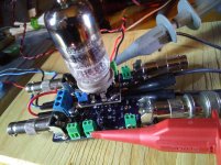
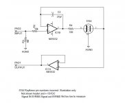
Well need some help here or at least some input.
This circuit has no visable anode supply. But it works better than anything I've tested. 8VRMS in 8VRMS out with distortion verrry low.
I have another thd measuring system at different location. Need to go pick it up.
Where are the electrons coming from?
This circuit has no visable anode supply. But it works better than anything I've tested. 8VRMS in 8VRMS out with distortion verrry low.
I have another thd measuring system at different location. Need to go pick it up.
Where are the electrons coming from?
Attachments
Pura Vida jfetter,
The electrons boil off the cathode and if they see a positive anode voltage they are accelerated towards it. The input of the buffer connected to the anode might present a DC voltage thus enabling the thing to work... can you decouple the triodes anode to the buffer with a 1uF non polarized cap?
I bet that would make it not work anymore.
Silviu
Pura Vida jfetter,
The electrons boil off the cathode and if they see a positive anode voltage they are accelerated towards it. The input of the buffer connected to the anode might present a DC voltage thus enabling the thing to work... can you decouple the triodes anode to the buffer with a 1uF non polarized cap?
I bet that would make it not work anymore.
Silviu
Savu , It lives! And still with incredible low distortion...?
10uF 50v BP now isolating anode.
Last edited:
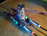
Here is a pic. Hi-res zoom in to see each part as on schematic.
Pura Vida, I like that. Costa Rica has strict privacy laws so I told my phone its native country Costa Rica.
Then Cortana audio monitor disappears from apps.
No other way to disable.
Pura Vida, I like that. Costa Rica has strict privacy laws so I told my phone its native country Costa Rica.
Then Cortana audio monitor disappears from apps.
No other way to disable.
Attachments
Well need some help here or at least some input.
This circuit has no visable anode supply. But it works better than anything I've tested. 8VRMS in 8VRMS out with distortion verrry low.
I have another thd measuring system at different location. Need to go pick it up.
Where are the electrons coming from?
When you say that this circuit works better than anything else you've tested, in what way do you mean that? I assume that your report of low measured distortion is also accompanied by some sort of unique subjective sound produced by the triode in the feedback loop? Can you elaborate? Thanks.
When you say that this circuit works better than anything else you've tested, in what way do you mean that? I assume that your report of low measured distortion is also accompanied by some sort of unique subjective sound produced by the triode in the feedback loop? Can you elaborate? Thanks.
Pura Vida Mr Ken.
I'll explain my statement, the quest being low conventional(thd marketed) distortion but with minimal components and safe construction.
From listening experience, I've found that a valve/tube within the audio chain always makes things 'sound' better. Somehow the tube corrects the golden ratio of odd even harmonics.
The circuit shown above injects the least poison(resistors-capacitors-iron) and maintains low thd, dc, phase and signal integrity. Hence "best ever".
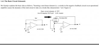
Here is a link with similar ideas; Mr. Shin-ichi Kamijo's concept. I have no connection with the site.
EN STC Super Triode Connection Power Amplifier
Bruce
Attachments
Last edited:
Pura Vida Mr Ken.
I'll explain my statement, the quest being low conventional(thd marketed) distortion but with minimal components and safe construction.
From listening experience, I've found that a valve/tube within the audio chain always makes things 'sound' better. Somehow the tube corrects the golden ratio of odd even harmonics.
The circuit shown above injects the least poison(resistors-capacitors-iron) and maintains low thd, dc, phase and signal integrity. Hence "best ever".
Bruce
Objectively, what THD fgures are you getting from your circuit. I should think that the triode is highly non-linear with such low voltage across it. That said, I am genuinely curious about it's subjective sound character. For instance, does it remind you of any particular commercial tube gear you've heard? Does it seem to combine the best of tube and solid-state sound? What about the sound do you dislike, if anything? Etc.
Thanks.
- Status
- This old topic is closed. If you want to reopen this topic, contact a moderator using the "Report Post" button.
- Home
- Source & Line
- Analog Line Level
- DOA - Discrete Op Amps