Hi Pals,
Few months ago I started this journey with B1 buffer stage. A simple and successful design by Mr.Pass.
Further research lead me to Feucht buffer.
Then I got tips from EUVL's design which basically a version of Feucht buffer without tracking capabilities.(My understanding,but may not be true!)
So after few weekends here I am with this design.
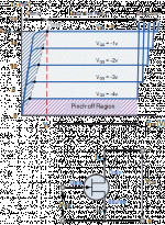
So the disadvantage of B1: running the jfet's at saturation, there is not much voltage swing to play with before distortion products goes up .
EUVL design (post #5 ) runs them at lower ID gives a little more headroom.
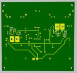
B1-Turbo on a Chip
Now being running at or near saturation B1 has an inherent advantage of PSRR. But when jfets working below Idss means they need very good power supply else power supply ripple will be transferred to audio signal.
Now being said all these, I took an excellent power supply design by Jan Didden (with his permission) and made this buffer stage that basically is EUVL's design from Feucht's.
Since this design uses BF862 and running them near 80%-90% of Idss means - cooling. It is challenging to cool this rice grain sized fets. They are thermally coupled through their gate pin. But to dissipate near 250mW(18V supply at 13ma Id) the area of 1oz copper pad needed is few square centimeters. You can glue a small heatsink on to them but those glues are much less efficient in heat transfer.
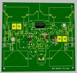
So here I am with this design ,I am planning to use small copper squares and fix them to board using nylon screws with heatsink paste between the copper squares.Nylon is not going to melt before 200C and before that jfets will go into smoke.
But to thermally track coupled JFET devices I will still use a small copper wire glued to them on top( or rather bolt them if I can work around HOW to do it,provided M1 screw hole for it).Well all this is to reduce Dc offset which is blocked by a nice capacitor at output.
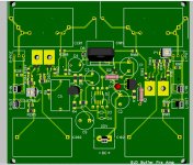
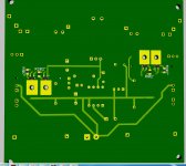
On board there is a trim pot to use as a single Feucht buffer which will dial down both source resistors to match. 0806 and 0603 options covers together a lot of 0.1% smd thin film combinations.
If you want to increase current for driving longer cables etc use the EUVL route by parallel use of 2 matched pairs of JFETS (on both sides of PCB).But SKIP the trimmer. Assuming you will use a nice cap at output to block any DC offset.
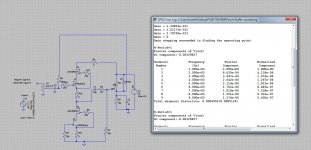
The output impedance should be in 20ohm range. Simulation shows predominant second harmonics with tad bit lower distortion figures than B1 design. But magnitude is in 10x-7so does not matter.
Let me know your thoughts.....
Few months ago I started this journey with B1 buffer stage. A simple and successful design by Mr.Pass.
Further research lead me to Feucht buffer.
Then I got tips from EUVL's design which basically a version of Feucht buffer without tracking capabilities.(My understanding,but may not be true!)
So after few weekends here I am with this design.
So the disadvantage of B1: running the jfet's at saturation, there is not much voltage swing to play with before distortion products goes up .
EUVL design (post #5 ) runs them at lower ID gives a little more headroom.
B1-Turbo on a Chip
Now being running at or near saturation B1 has an inherent advantage of PSRR. But when jfets working below Idss means they need very good power supply else power supply ripple will be transferred to audio signal.
Now being said all these, I took an excellent power supply design by Jan Didden (with his permission) and made this buffer stage that basically is EUVL's design from Feucht's.
Since this design uses BF862 and running them near 80%-90% of Idss means - cooling. It is challenging to cool this rice grain sized fets. They are thermally coupled through their gate pin. But to dissipate near 250mW(18V supply at 13ma Id) the area of 1oz copper pad needed is few square centimeters. You can glue a small heatsink on to them but those glues are much less efficient in heat transfer.
So here I am with this design ,I am planning to use small copper squares and fix them to board using nylon screws with heatsink paste between the copper squares.Nylon is not going to melt before 200C and before that jfets will go into smoke.
But to thermally track coupled JFET devices I will still use a small copper wire glued to them on top( or rather bolt them if I can work around HOW to do it,provided M1 screw hole for it).Well all this is to reduce Dc offset which is blocked by a nice capacitor at output.
On board there is a trim pot to use as a single Feucht buffer which will dial down both source resistors to match. 0806 and 0603 options covers together a lot of 0.1% smd thin film combinations.
If you want to increase current for driving longer cables etc use the EUVL route by parallel use of 2 matched pairs of JFETS (on both sides of PCB).But SKIP the trimmer. Assuming you will use a nice cap at output to block any DC offset.
The output impedance should be in 20ohm range. Simulation shows predominant second harmonics with tad bit lower distortion figures than B1 design. But magnitude is in 10x-7so does not matter.
Let me know your thoughts.....
Attachments
Last edited:
Hi Pals,
Few months ago I started this journey with B1 buffer stage. A simple and successful design by Mr.Pass.
Since this design uses BF862 and running them near 80%-90% of Idss means - cooling.
0806 and 0603 options covers together a lot of 0.1% smd thin film combinations.
But SKIP the trimmer. Assuming you will use a nice cap at output to block any DC offset.
Let me know your thoughts.....
Hmm...my thoughts.
First, as you stated the B1 may be a successful design by Mr. Pass, but all my examples both AC and DC-coupled have resulted in less-than-stellar SQ.
Adjectives such as "sterile" and "lifeless" come to mind.
ANY design that uses only 2 devices(JFET or BJT) per channel is going to result in $h_tty SQ.
Unfortunately, the old design philosophy that "simpler is better" just doesn't seem to apply to any 2-4 transistor designs that I've tried.
Second, I wouldn't run those cheesy little BF862s at 80-90% of their Idss rating unless you're desiring to shorten their lives and have one or more of them to self destruct.

Third, if you enjoy soldering 0806 and 0603 SM resistors, I say "Go for it Dude".
I won't attempt to solder anything smaller than 1206 and there are plenty of .1%(not that it really matters for this design) thin film resistors in that larger size.
Fourth, rather than use a "nice cap" at the output, why don't you figure out how to better match the devices so that NO cap is needed at the output.
Remember, coupling caps blow and should always be avoided if possible.

Now...let's bust out the moonshine and soldering iron and build something!
Cascode will remove the high dissipation concern of the very small 862 and will help with PSRR.
Each device (4 in total for a paralleled CCS+Follower) needs it's own selected source resistor to try to get Id for each close to identical. Close enough may be trimmers of the lower Rs on both halves. When output offset becomes zero for one half, then you know that Id for that half has been set up accurately.
My eyes need reading glasses, and I have soldered 805/603/402 with optical aids without any real problem.
Last edited:
Could you explain?..............
Remember, coupling caps blow and should always be avoided if possible....................
Ammel, valid points. But remember this is just a buffer and so is B1. There are lot of satisfied people who use them. What was the potentiometer type you used in your design? What cables you used ?
Running them at 90% of Id may not be an issue of they are properly heatsinked. They are rated for 300mW and even at full Idss they only reach 270
-290 mW if you chose Less than 16 Idss devices. Not sure running a transistor hot necessarily means a short life span, it is a relative concept. Unless you have ran them in both ways with enough sample size it is just an observation from you.
Soldering 0603 may be a challenge but 0805 is not for most people. Well we are taking about using soldering paste and SMD soldering station. You can buy them for less than 60$ from Amazon . Most of us will spend double the money buying boutique components for our carnal pleasures. If you have not it is kind of late, don't you think?
No caps is still possible if you have perfectly matched Jfets not just IDSs and Vp . Do you know how to use a curve tracer ? Most people here don't . And doing that with SMD should be challenging too. A cap in signal path is not a dreaded thing to have.
We should stop thinking soldering SMD parts using regular iron , yes it is a mess. I don't think even soldering those Jfets with a regular iron is easy.1206 package is better but also expensive( again relative word). But defenitely a good suggestion. When I searched it was easier and cheaper to find 0805 and 0603 at mouser with lot more options.
Andrew thanks for suggestions. Yes all the source resistors are independent. I thought about using a trimmer for both sides. But practically it is tough to access both sides of the board and also may make it challenging to fine tune. Also Feucht paper recommend using only 1% matched resistors and with SMD resistors we have 0.1% available.
thank you guys.
Last edited:
Excuse me Ammel - but what is "SQ"?
I believe it is Sound Quality!
Hi,
soldering the BFs SOT23 casing should be no more difficult than soldering a TO92 throughhole transistor .... they share almost same pad sizes and distances.
The problem with temperature and JFETs is gate leakage.
Unfortunately gate leakage is often not or grossly unpractically specified in Datasheets.
Running JFETs at high Id and high temperature condition lets the leakage rise over due.
If the gate resistor is chosen large (quite often 1M and more) the rising leakage can drive the JFET into a latch up, or in other words destruction.
As a rule of thumb the drain-source voltage should not exceed 1/4 of the specced max value when You intend to run the JFET 'hot'.
If You can't reduce the supply rails then cascoding is a option -also reducing THD considerably- or adding a power booster (Darlington or Sziklai) and reducing the JFETs Id.
The latter case is what I did in my Calvin Buffer .... allowing to bias the JFET lower, close to its 0-tempco point, and still benefitting from the current drive capabilities of a bipolar booster transistor.
No need for a parallel configuration and the hassle with trimming 4 or more bias currents to match.
jauu
Calvin
ps. never seen a coupling cap blow up ..... must be another one of those highend fairytales
Thank Calvin. Appreciate your comments. Always nice to hear from you.
I will take my comments back on soldering those jfets,I should have rather said handling than soldering.
I have chosen 200R for gate resistance.
Now about running hot, So these jfets pump out heat through their gate pins than over there slender bodies, is that correct?
I found this calculator
The CircuitCalculator.com Blog >> PCB Thermal Copper Area
Attached screen shot of my calculation. So it needs about 500 square mm of 1.4mils(0.036mm) copper pad to keep junction temp at 60degrees.
My pad area is about 40 mm square, but heat sinking fortunately is a volume issue. So assuming 18 cubic mm of copper pad (500 x 0.036) can keep the junction at 60degree ,I can use a 0.5 mm copper plate and get more volume for cooling (40mmx0.5=20 cubic mm). Ok will use two 0.5 mm copper plates making it double the volume(40) to cool!
I definitely has plans to make your buffer Calvin. But this design only uses local feed back and all others including yours uses global feedback, am I right?
Not sure how to cascode Jfets into a buffer. If anyone has a circuit with bf862 happy to adapt it.

Hi,
my Buffer only relies on local feedback.
The JFET Master and the bipolar Slave in Sziklai configuration form a highly linear 'supertransistor' due to the very short, direct local feedback.
But since the circuit topology consists of only these two transistors the local feedback could be regarded as global feedback loop at the same
You can use the BF862 in that configuration too ..... there's already been a thread showing a small PCB layout for the Buffer utilizing the BFs.
jauu
Calvin
Last edited:
Hi,
If You can't reduce the supply rails then cascoding is a option -also reducing THD considerably-
Calvin I guess I understand what you are saying now.
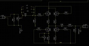
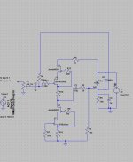
Cascode is the way ,SST4391 is obsolete, so I used MMBF4391.
Can we use same JFET in all 4 positions? When I did it gave me significant THD figures.
And this one is considered local feed back?
Attachments
Last edited:
This part I did not understand well.You can use the BF862 in that configuration too ..... there's already been a thread showing a small PCB layout for the Buffer utilizing the BFs.
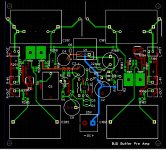
While waiting for Calvin to reply ,I made the changes. Not sure matching the lower resistors with upper, like Feucht recommended still apply to cascode.
Also provided pads for 1206 resistors for shaky hands
Also provided pads for 1206 resistors for shaky hands
Attachments
the cascode transistor should be a high Vpinchoff device.
And to get a high voltage across the follower it also needs to be high Idss.
If you are using 12mA bf862, then I suggest you look at Idss for the cascode >24mA and when this cascode is passing 10mA (~90% of 12mA Idss) the Vgs should be >2* Vpinchoff of the 862.
You can measure your cascode to achieve this. Pass 10mA through it with a VR in it's source and measure the Vgs. You want at least 1.5Vgs, preferably >2V since this becomes the Vds of the Follower.
Excuse me Ammel - but what is "SQ"?
Sorry...Sound Quality.
Could you explain?
Andrew, as long as you've been on this site and as many posts you've replied to, you would be one of the last members I expect to not understand such a simple statement.
my Buffer only relies on local feedback.
The JFET Master and the bipolar Slave in Sziklai configuration form a highly linear 'supertransistor' due to the very short, direct local feedback.
But since the circuit topology consists of only these two transistors the local feedback could be regarded as global feedback loop at the same
Having built several examples of Calvin's Buffer, I can attest to the fact that it sounds really good.
In fact, it's probably my favorite discrete buffer even though it uses many more components than Nelson's B1.
I like it so well that I designed my own PCB for it, which uses only through-hole components.
I use PF5102 and J107 JFETs which I match myself.
Sorry kinku for the slight thread derailment.
When you get your PCBs back for your B1 version of Feucht buffer, please keep us posted on how it turns out.
- Status
- This old topic is closed. If you want to reopen this topic, contact a moderator using the "Report Post" button.
- Home
- Source & Line
- Analog Line Level
- BJD BUFFER stage for passive preamps