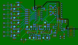
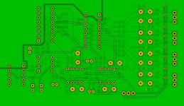
Hi, I'm currently in the process of laying out my PGA2310 preamp pcb. I've done analog part so far and only digital connections to the board and mute relay driver left but digital connections are easy stuff to layout I think.
The circuit goes like this: (4 inputs with RF filters) -> (DG409 input switch) -> (inverting buffer with dc servo(second half of OPA2134)) -> (PGA2310 volume regulator) -> (inverting buffer to bring phase back to normal) -> (output (with mute relay))
I've read a lot of recommendations and data sheets on the PCB design but it's my first PCB and I would appreciate any critics and comments on the design.
Thank you.
P.S. Why I used smd capacitors and resistors but through hole chips is because I already have these chips. I've built the circuit on breadboard first. And PGA2310 alone costs around 30 EUR so I don't want to just throw it away.
Attachments
Last edited:
A schematic would not hurt for a review
1) 22K in series with the DG409, why?
2) sot-23, across the supplies?
Unfortunately I don't have the schematics in digital form but will try to draw it soon.
1) 22k resistors is the input series resistors for inverting buffer that comes after DG409. Together with 22k in opamp's feedback forms a regular inverting circuit.
2) sot-23 is a pair of diodes on the input to prevent static electricity getting into IC
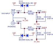
Basically input stage is the copy of input of one commercially available amp except that I've replaced 2 separate DG408 to a stereo DG409. I've attached schematics of that amp.
Attachments
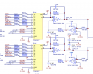
Looks like a reasonable design. A few details to check - I noticed that the + input terminals on U5.2 and U5.1 are not connected. Tie them to ground. Also, if U2.3, U3.3 and U5.3 are unused, tie their inputs to ground as well - even better, tie output to -input and +input to ground. That might be an artifact of the incomplete drawing that you warned about, but still U5.1 and U5.2 need to be checked.
Looks like a reasonable design. A few details to check - I noticed that the + input terminals on U5.2 and U5.1 are not connected. Tie them to ground. Also, if U2.3, U3.3 and U5.3 are unused, tie their inputs to ground as well - even better, tie output to -input and +input to ground. That might be an artifact of the incomplete drawing that you warned about, but still U5.1 and U5.2 need to be checked.
U2.1, U2.2 and U2.3 are parts of the same chip U2 displayed separately for convenience. So all op amps' inputs are connected. The only thing I've missed is the connection on pins 5 and 3 of U5 to ground, but on pcb they are connected to ground.
What are you using to control this pre-amp?
I have some BASCOM-AVR code to offer for this type of design. Written for a Atmel xmega mcu, a character LCD, bourns encoders. Also have code for IR remote too.
Why not use NPO/COG MLCC caps for i/p filters instead of TH?
Why not place the RCA i/p jacks on the pcb? I like designing stuff that uses minimal wiring.
What ecad s/w are you using? Now I see EasyEDA, in the sch title block. I can review your gerber/drill data once you are done.
10uF filter caps could be MLCC instead of tantalum = more reliable, lower ESR, cheaper too.
Could also place some small R(100-600) at the o/p of U5 before the relays. I do wonder what it will sound like(pop/shock noise) if you directly short these o/p's. the PGA2310 mute function might be sufficient without resorting to the relay technique. Always nice to have options available when prototyping
Last edited:
What are you using to control this pre-amp?
I have some BASCOM-AVR code to offer for this type of design. Written for a Atmel xmega mcu, a character LCD, bourns encoders. Also have code for IR remote too.
Why not use NPO/COG MLCC caps for i/p filters instead of TH?
Why not place the RCA i/p jacks on the pcb? I like designing stuff that uses minimal wiring.
What ecad s/w are you using? Now I see EasyEDA, in the sch title block. I can review your gerber/drill data once you are done.
10uF filter caps could be MLCC instead of tantalum = more reliable, lower ESR, cheaper too.
Could also place some small R(100-600) at the o/p of U5 before the relays. I do wonder what it will sound like(pop/shock noise) if you directly short these o/p's. the PGA2310 mute function might be sufficient without resorting to the relay technique. Always nice to have options available when prototyping
I'm using Arduino Nano to control the preamp. All code is already written for it including LCD, IR, encoders.
For input I've copied one commercial amp and it uses film capacitors here. This is the main reason. AFAIK capacitance of film capacitors is more stable through frequency range than ceramics and it's important in filters. Is it true?
I thought about placing RCAs on the board and it makes the most sense, I understand that. However I decided to stay with wiring for now to have more freedom with mounting inside the enclosure. I might consider actually putting RCAs back on the board. However one of the inputs will be connected by wires anyway because it will come from DAC mounted in the same enclosure.
I've used EasyEDA only for schematics. For laying out PCB I've used Sprint Layout 6.
I've used 10uF tantalum caps here as it is stated in the PGA2310 data sheet as the decoupling solution. Maybe they just used the cheapest caps that do the job, I don't know. Just used what was in the data sheet for IC.
According to OPA2134 data sheet it is short circuit "friendly". However I just checked the schematics of commercial amp that I've mentioned before and they indeed have 47R resistors between IC and relay. I will also put it there. However I've evaluated solution on a breadboard and it works without clicks and pops.
Mute pin of PGA2310 is not sufficient to eliminate of/off thump which is nasty with this IC. I've tried a lot of solutions for muting and relay one appeared to be the most reliable way to do this. It allows to make muted state the default even with no power. Signal from Arduino is needed to unmute the circuit in this case. There was a separate thread n this forum where I was fighting this thump.
Keep in mind that I'm just a novice hobbyist so everything I wrote is based on my current basic knowledge and "beliefs"
") and I don't claim it to be true so any critics that I can use to learn something new is appreciated.
and I don't claim it to be true so any critics that I can use to learn something new is appreciated.Thank you very much for your help.
Some random thoughts...they may or may not help!
Circuit is a little unusual, looks like the inputs switches are inside the input/feedback circuit on the opamp. You have multiple 22k resistors on the DG409 input. I would have put one 22k on the DG409 output and remove the other 22k, or replace with 0R resistors. I guess without any other reference to ground on the op-amp, given the 100nF on the positive pin to ground, that when the DG409 switches or when you power on/off it might make the on/off thump worse? Just a guess though and could be wrong.
U5.1 and U5.2 really need series resistors in the outputs (47 to 100ohms) if they are driving cables.
The integrators are interesting instead of using DC blocking caps, although you may still end up with some small offset voltage on the output which may be an issue depending on what you are driving with the outputs.
Film capacitors will be better at the values you are using that equivalent ceramics (X7R/X5R which change over voltage, frequency etc). Tantalum capacitors will be fine but they tend to be more expensive, any 10uF-100uF aluminium electrolytic would work as well.
I mention " NPO/COG MLCC caps for i/p filters instead of TH" since they are very stable. It is the (X7R/X5R which change over voltage, frequency etc) that are not recommended for reasons stated.
I guess you have to use what you have too, fine for making your own pcb's but tools like " Sprint Layout 6." irc have no DRC checking, linkage to schematic, so can be error prone.
ohdsp makes a good point about " I would have put one 22k on the DG409 output and remove the other 22k, or replace with 0R resistors."
Circuit is a little unusual, looks like the inputs switches are inside the input/feedback circuit on the opamp. You have multiple 22k resistors on the DG409 input. I would have put one 22k on the DG409 output and remove the other 22k, or replace with 0R resistors. I guess without any other reference to ground on the op-amp, given the 100nF on the positive pin to ground, that when the DG409 switches or when you power on/off it might make the on/off thump worse? Just a guess though and could be wrong.
The integrators are interesting instead of using DC blocking caps, although you may still end up with some small offset voltage on the output which may be an issue depending on what you are driving with the outputs.
Film capacitors will be better at the values you are using that equivalent ceramics (X7R/X5R which change over voltage, frequency etc). Tantalum capacitors will be fine but they tend to be more expensive, any 10uF-100uF aluminium electrolytic would work as well.
Preamp will be driving power amp in the integrated amplifier that has 2uF dc blocking caps on input.
As for thump because of 100n cap, honestly I have no idea how it will affect power on thump but since there's a relay on the output of preamp, there's no way that thump will get into power amp.
I mention " NPO/COG MLCC caps for i/p filters instead of TH" since they are very stable. It is the (X7R/X5R which change over voltage, frequency etc) that are not recommended for reasons stated.
I guess you have to use what you have too, fine for making your own pcb's but tools like " Sprint Layout 6." irc have no DRC checking, linkage to schematic, so can be error prone.
ohdsp makes a good point about " I would have put one 22k on the DG409 output and remove the other 22k, or replace with 0R resistors."
I thought that even NPO are not that stable as film capacitors. Good to know that they can be used for the filters. I'll think I'll go with them then. It will save a lot of space and make layout easier. Can they also be used in servo circuit instead of film capacitors? (0.47uF in the feedback and 100n between the positive input and the ground)
As for multiple 22k resistors I actually copied it from the schematic that I've posted above. I also was quite surprised that they used 16 22k resistors at the inputs of a switch IC instead of just 2 at the outputs and also would like to know why is that.
Circuit is a little unusual, looks like the inputs switches are inside the input/feedback circuit on the opamp. You have multiple 22k resistors on the DG409 input. I would have put one 22k on the DG409 output and remove the other 22k, or replace with 0R resistors.
It's a good plan. He's switching current, not voltage, by loading the switches into a virtual earth and by using the 22kΩ resistors ahead of the switch to drop the voltage. This greatly reduces the voltage swing across the solid state switch and greatly reduces distortion. It also allows you to use potentially low voltage switching chips with professional level signals. The only gotcha to this is that the VE amp gets de-stabilized from the switch capacitance, but you can easily compensate that with the feedback cap C5 that he has on the shown schematic.
Solid state switches should be used either switching only current with no voltage swing (loading them into a virtual ground) or by switching only voltage with no current passing through (loading into a very high Z input, like an op amp input terminal). Anything between the two extremes will result in extra distortion.
I thought that even NPO are not that stable as film capacitors. Good to know that they can be used for the filters. I'll think I'll go with them then. It will save a lot of space and make layout easier.
NP0 / C0G caps are great for filtering uses, if you can tolerate their small capacitance. I have measured the distortion of some Murata 100nF C0G MLCCs and they're quite clean. They start to show signs of saturation only about 10dB earlier than a 100nF 200V Component Research Teflon film and foil cap, and those are pretty fantastic caps. By 'fold up', that means slightly peeking above the distortion floor of an APx-555, which for these tests is around 150dB below the 5V peak drive signal with about 5mA peak current passing through it. Many film caps will do worse than either the CRC or Murata caps, FWIW.
Can they also be used in servo circuit instead of film capacitors? (0.47uF in the feedback and 100n between the positive input and the ground)
Yes, they're great for servos. They're low cost, non microphonic, their small size leads to small parasitics and less unwanted coupling to other parts of the circuit, they're stable, and have a very low temperature coefficient, unlike many films.
You'll have a hard time finding a 470nF C0G, but they do exist. You can also use a resistive divider after the servo's output lowpass filter (R9/C6) to reduce the loop gain of the servo. This has the effect of lowering the corner frequency, allowing you to use smaller caps, and it also attenuates noise from the servo amp, at the expense of a narrower range of DC offset correction. The OPA2134 has an output range of ±13V, and you surely don't need to correct that much DC ever, so it's a good tradeoff.
I find LTspice useful in tuning DC servos - juggling the gains and turnover frequencies gets a little unnerving, and a good simulation will do the math for you very accurately. You can also see if there are any passband aberrations caused by the servo that can be tuned away by adjusting your two stage filter.
Last edited:
It's a good plan. He's switching current, not voltage, by loading the switches into a virtual earth and by using the 22kΩ resistors ahead of the switch to drop the voltage. This greatly reduces the voltage swing across the solid state switch and greatly reduces distortion. It also allows you to use potentially low voltage switching chips with professional level signals. The only gotcha to this is that the VE amp gets de-stabilized from the switch capacitance, but you can easily compensate that with the feedback cap C5 that he has on the shown schematic.
Solid state switches should be used either switching only current with no voltage swing (loading them into a virtual ground) or by switching only voltage with no current passing through (loading into a very high Z input, like an op amp input terminal). Anything between the two extremes will result in extra distortion.
Now it starts to make sense why they used resistors at the input of switches. Thank you for explanation. Do I get it right that if resistors would be placed after switch then there would be a voltage drop across the switch and because of imperfection of the switch it would introduce distortion? Or is there some other reason why distortion would be higher? I'm trying to learn all I can so might ask stupid questions.
Also about stability I still don't fully understand what contributes to instability of op amp and why and how certain elements (like cap in feedback) compensate for it. Where can I find some materials that can explain that starting from basics. I've seen quite a bit of articles and other stuff explaining stability but they are based on some knowledge that I unfortunately don't have. So when I try to read those materials I quickly stop understanding what is written there.
Yes, they're great for servos. They're low cost, non microphonic, their small size leads to small parasitics and less unwanted coupling to other parts of the circuit, they're stable, and have a very low temperature coefficient, unlike many films.
You'll have a hard time finding a 470nF C0G, but they do exist. You can also use a resistive divider after the servo's output lowpass filter (R9/C6) to reduce the loop gain of the servo. This has the effect of lowering the corner frequency, allowing you to use smaller caps, and it also attenuates noise from the servo amp, at the expense of a narrower range of DC offset correction. The OPA2134 has an output range of ±13V, and you surely don't need to correct that much DC ever, so it's a good tradeoff.
I find LTspice useful in tuning DC servos - juggling the gains and turnover frequencies gets a little unnerving, and a good simulation will do the math for you very accurately. You can also see if there are any passband aberrations caused by the servo that can be tuned away by adjusting your two stage filter.
I've searched for 0,47uF C0G caps at my supplier and was able to find one but they come for ridiculous price of 16 EUR per 1 cap. Also the come only in huge 2220 package. So I'll stick with film here. With 0,1uF C0G caps it's a bit better though.
It's a good plan. He's switching current, not voltage, by loading the switches into a virtual earth and by using the 22kΩ resistors ahead of the switch to drop the voltage. This greatly reduces the voltage swing across the solid state switch and greatly reduces distortion. It also allows you to use potentially low voltage switching chips with professional level signals. The only gotcha to this is that the VE amp gets de-stabilized from the switch capacitance, but you can easily compensate that with the feedback cap C5 that he has on the shown schematic.
Solid state switches should be used either switching only current with no voltage swing (loading them into a virtual ground) or by switching only voltage with no current passing through (loading into a very high Z input, like an op amp input terminal). Anything between the two extremes will result in extra distortion.
Interesting idea for pro level signals; However if this was not needed and given the low current in this application as it is feeding a FET input op-amp I assume the difference in distortion from moving the DG409 before the op-amp stage should make little difference.
And wouldn't the longer track work and additional components on the op-amp input pins increase the noise levels?
Would it not make sense to put the i/p clamp diodes (BAV99) after the 1k i/p R's(R1,3), that way they have some current limiting capability. As they are, depending on the source Z &/or its current limiting capabilities they could blow in case they are made to conduct.
"given the low current in this application as it is feeding a FET input op-amp"
that would be the case if it was in a non-invert config, but it is a inverting design so it see a 2k load due to the virtual ground.
"given the low current in this application as it is feeding a FET input op-amp"
that would be the case if it was in a non-invert config, but it is a inverting design so it see a 2k load due to the virtual ground.
Interesting idea for pro level signals; However if this was not needed and given the low current in this application as it is feeding a FET input op-amp I assume the difference in distortion from moving the DG409 before the op-amp stage should make little difference.
Yes, the same buffer amp could be used as an inverter in a VE switching mode, or as a follower in a voltage only switching mode, but inverting stages are inherently cleaner, especially with FET input op amps.
The input FET pair of the op amp is generally implanted into a junction well. This makes the JFET drain to substrate parasitic capacitance vary with the op amp common mode signal. In a non-inverting stage, the entire signal appears as common mode to the op amp, so the capacitance modulation is greatest. If you're very unlucky, you can get buckets of 2nd harmonic distortion that rises with frequency at 6dB/octave. For details, read these: http://www.ti.com/lit/an/slyt595/slyt595.pdf and Analog's AN-232: http://www.analog.com/media/en/technical-documentation/application-notes/742022599AN232.pdf
The common mode signal voltage of an op amp configured as an inverter is essentially zero, so this common mode distortion mechanism does not manifest itself.
There are some other squirrely substrate junction and limited PS voltage issues with the old 4000 series CMOS switches as well, (which don't apply to the DG409), so that's another reason why I generally favor the VE current switching approach.
I've been working with solid state audio switching circuits for a few years, and if you do it right, an entire VE current mode switch, including the amplifiers, can be made with the only measurable distortion being second harmonic at around -152dBc, barely a few dB above the test set floor. By comparison, a single OPA1642 follower will yield -142dBc 2kHz distortion without switches, and other amps will do a lot worse. Plus, with the VE circuit, you can use bipolar op amps, which are generally cleaner than FET amps anyway.
Whether you care about distortion that low is another matter, but by comparison, the VE circuit is measurably better, and all you did was stir around the circuit a bit, using the same parts, and a few extra resistors.
And wouldn't the longer track work and additional components on the op-amp input pins increase the noise levels?
No increase of noise, but an increase of shunt capacitance, which can be compensated for.
Now it starts to make sense why they used resistors at the input of switches. Thank you for explanation. Do I get it right that if resistors would be placed after switch then there would be a voltage drop across the switch and because of imperfection of the switch it would introduce distortion? Or is there some other reason why distortion would be higher? I'm trying to learn all I can so might ask stupid questions.
That's exactly right, and there are no stupid questions, except those un-asked! All solid state switches vary their 'on' resistance with voltage across the drain-source channel, which depends upon the current through the switch. This would seem to favor voltage switching, in order to eliminate current, but in analog switch ICs, they use a back-to-back series pair of FETs to counteract this, and if the two devices match, as they do on an IC, this effect completely cancels. When switching voltage in an analog switch IC, the D-S channel to substrate capacitance biasing voltage, which is the switched signal, modulates the depletion layer depth in the D-S channel, and thus modulates the on resistance of the switch. This effect can only be compensated for by bootstrapping the substrate voltage so the D-S to substrate voltage is now constant, but that makes controlling the gate-source drive voltages of the switching FETs really annoying, requiring yet another op amp in the ideal case.
So, by dropping almost all of the signal voltage ahead of the switch, except the tiny bit left dropped across the switch itself, you use a much smaller part of the Rdson vs. voltage curve, and it's much cleaner. And, if you use a series back-to-back switch FET pair, the current effects completely cancel, as long as the switch FETs are matched, which happens easily in a switch IC. This means that current mode is generally best for an IC analog switch. With discrete switch transistors, you can avoid the substrate parasitic junction entirely, and you can also choose possibly better devices, but it gets much more complicated, pretty quickly.
Also about stability I still don't fully understand what contributes to instability of op amp and why and how certain elements (like cap in feedback) compensate for it. Where can I find some materials that can explain that starting from basics. I've seen quite a bit of articles and other stuff explaining stability but they are based on some knowledge that I unfortunately don't have. So when I try to read those materials I quickly stop understanding what is written there.
The simplest way to view it is to see that a capacitance from the op amp -input node to ground forms a lowpass filter on the feedback signal from the op amp output through the feedback resistor to the -input. This means that the feedback goes away at very high frequencies, making the amp unstable. If you add a capacitor across the feedback resistor, it compensates for the input shunt capacitance by reducing the feedback resistor's impedance as frequency rises, and counteracting the rolloff of the feedback signal from output to the -input. So, loosely speaking, if the feedback cap matches the input shunt cap, the effects of the shunt cap go away. There's a limit to this compensation, since the amplifier is now driving two caps in series to ground, and that will annoy the op amp's output stage, making it unstable, but many amps will cope with 10-100pF to ground without becoming unstable.
Probably the best thing to read about the basics is The Art of Electronics by Horowitz and Hill. The new 4th edition is really great, with a lot of updates and practical info that can apply to audio circuits. Basic circuit theory is a big topic, but it's not impossible to tackle.
I've searched for 0,47uF C0G caps at my supplier and was able to find one but they come for ridiculous price of 16 EUR per 1 cap. Also the come only in huge 2220 package. So I'll stick with film here. With 0,1uF C0G caps it's a bit better though.
Yeah, large C0G caps cost a fortune and are huge, but they're still tiny compared to a film and a lot cleaner, unless you spend a lot of money. Still, you do not need anything above 0.1µF for a servo - using an output attenuator to reduce the servo loop gain will lower the effective highpass frequency. In a servo I'm working on now, I'm using around 60K and 0.1µF, and I get an overall high pass corner of 1Hz because the servo output is attenuated back into the amplifier it's correcting. That also solves a lot of other problems, such as minimizing the servo amp's LF noise, which is injected back into the controlled op amp.
It's best to use a simulator like LTspice to verify the response of these circuits, since the calculations can get complicated, and at the very least, it's nice to have confirmation that what you think is happening is actually happening.
I think this is the input stage from an ARCAM A85 amplifier. I used to be the design manager there and think I recognise it.
I didn't design it so my memories of how it operates are second hand.
You are correct about how the opamp is set up to reduce common mode stress and the resistors being before the CMOS switch to reduce voltage variance across the switch and thus reduce distortion.
The BAV99 is before the resistor as it is intended to catch static events and can cope with the energy in this form. If you put it after the resistor the slight modulation of the reverse biased diode junction capacitance seemed to upset the sound. It is a compromise and you are right it would perform better as protection after the resistor.
The servo is very low frequency as we found that both the amplitude and phase changes due to it needed to be outside the audible range. I like the idea of the attenuator, however if you are going to AC couple into your power amplifier it might be easier to simply AC couple here as well. I seem to remember we had some problems with the occasional volume control not liking the slow DC settling.
We did listening tests on the differences between Film and COG capacitors and the results were not statistically valid but showed a slight preference for COG. Despite this due to the perceived better performance of film caps the company decided to stay with them. Personally I would be comfortable to change over to COG.
I would also like to second the recommendation to learn LTSpice, it has a very infuriating user interface however once mastered is extremely valuable for both checking calculations and iterating ideas quickly.
Best of luck with your design. Personally I would find yourself a Schematic capture and PCB layout solution that integrate together with net list transfer and error checking as you have a much much higher chance of getting the design right. Currently the Design Spark software that is free from RS components is one of the best free solutions. It is based on a slightly cut down version of the easyPC CAD package (However they have made the file formats incompatible). It is a full Schematic capture and design package with full error checking as such it is non trivial to learn however once you have learnt you will be able to design much more complex PCBs and use all the error checking tools to reduce design faults.
- Status
- This old topic is closed. If you want to reopen this topic, contact a moderator using the "Report Post" button.
- Home
- Source & Line
- Analog Line Level
- Laying out preamp pcb