Hi, I hope you had a good Christmas. Yes your first assumption is correct. The signal can be treated as terminating at the opamp and being regenerated at the output.
For a first build a two layer PCB is a good option. You really need more experience with CAD and a CAD package where the netlist is transferred from the schematic for a multilayer design.
I will try to track down an example of the different servo options so you can see what a second order servo means and does. I remember now sone of the reasons the designer went with first order was as the filter had to trade off frequency cut off with settling time and noise generated by the large resistors and group delay in the filter. He spent quite a long time on this part of the design and this was his best compromise in this application.
Regards
Andrew
Thank you. Unfortunately I don't know the theory behind the dc servos very well except the general principle and couldn't find simple enough explanation of it yet. I'm afraid that it will be a waste of your time to show different types of servo circuit as I won't be able to understand the difference

Bob Cordell covered servos in his power amp design book.
As said earlier, a useful resource is to learn/use LTspice, that way you can play with these servo designs and see what differences they make.
Post your DAC controller questions, we'll take a shot at answering them
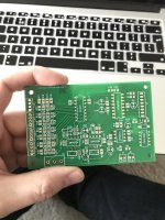
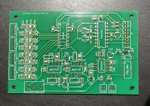
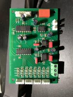
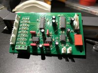
I've got DAC board based on CS4398 dac chip and CS8416 receiver chip. It has 2 optical and 2 coax inputs. The main thing to solve is to find out how to control CS8416 chip from Arduino for input selection and maybe reading and displaying of current audio format.
One more thing is to find out is what is CS4398 software mode, what is it used for and whether I need to control it.
I will control DAC chip via SPI because I already control PGA2310 and LCD display via it.
did you buy it or make it?I've got DAC board based on CS4398 dac chip and CS8416 receiver chip.
All your answers are in the data sheets and app notes, but i'll give a bit of help.
iirc 8416 has both hardware and software modes of operation, a dedicated pin to control sampled at the power on state.I've got DAC board based on CS4398 dac chip and CS8416 receiver chip. It has 2 optical and 2 coax inputs. The main thing to solve is to find out how to control CS8416 chip from Arduino for input selection and maybe reading and displaying of current audio format.
I suggest to get it going in h/w mode first and then learn to write the code to control it in s/w mode. I have to check the control interface, i think it is i2c and spi, it really does not matter which you use. atmega has hardware i2c and spi op. for spi you have to setup the configuration of which edge of the clock the data gets latched. if using i2c you have to determine the device address. then you have to look at the registers to figure out how to program them. there are registers for input selection and a whole bunch of other stuff.
for the dac cs4398, I will have to look at it as I am not too familiar with it as to what it uses for a interface. you say spi, so that is easy, you just need to elect mcu pins to act as spi slave selection control and use the common interface.
you have to check the logic level voltages involved. is the spi using a 5V supply? and what is the 4398,8416 running at. if the slaves can not accept 5V logic you have to level shift. this is why I do not like ardunio, most modules run at 5V and most slaves are 3V3 these days. I use xmega for that reason.
the dac would have registers for things like sample rates, digital data interface, selection, i2s, left/right justified etc.
if it was my design, i'd have as many separate spi i/f's as possible, one just for the display, as that is probably the most active, that way you keep the noise down for devices like the pga. mcu's are cheap, I like the xmega a1 and it derivatives.
hope this helps you.
P.S. i was thinking of building a spdif receiver and dac too, so i can play music on the PC and send it to my audio system. i might be able to do the same as you
Last edited:
did you buy it or make it?
All your answers are in the data sheets and app notes, but i'll give a bit of help.
iirc 8416 has both hardware and software modes of operation, a dedicated pin to control sampled at the power on state.
I suggest to get it going in h/w mode first and then learn to write the code to control it in s/w mode. I have to check the control interface, i think it is i2c and spi, it really does not matter which you use. atmega has hardware i2c and spi op. for spi you have to setup the configuration of which edge of the clock the data gets latched. if using i2c you have to determine the device address. then you have to look at the registers to figure out how to program them. there are registers for input selection and a whole bunch of other stuff.
for the dac cs4398, I will have to look at it as I am not too familiar with it as to what it uses for a interface. you say spi, so that is easy, you just need to elect mcu pins to act as spi slave selection control and use the common interface.
you have to check the logic level voltages involved. is the spi using a 5V supply? and what is the 4398,8416 running at. if the slaves can not accept 5V logic you have to level shift. this is why I do not like ardunio, most modules run at 5V and most slaves are 3V3 these days. I use xmega for that reason.
the dac would have registers for things like sample rates, digital data interface, selection, i2s, left/right justified etc.
if it was my design, i'd have as many separate spi i/f's as possible, one just for the display, as that is probably the most active, that way you keep the noise down for devices like the pga. mcu's are cheap, I like the xmega a1 and it derivatives.
hope this helps you.
P.S. i was thinking of building a spdif receiver and dac too, so i can play music on the PC and send it to my audio system. i might be able to do the same as you
I bought the board from another DIYer. It is a good point about logic levels. I've checked data sheets for both CS4398 and CS8416 and both of them can be configured to run on 3.3V or 5V, they have separate VDL reference voltage pins for this purpose. I've checked the schematic of the board that I have and can see that it it is configured to run on 5V logic levels so no problem with arduino here.
I've checked the data sheet for 4398 and can see that it can be configured for different data formats. Currently it is configured in hardware mode Dual-Speed I2S. I still need to find out what does it mean for me and what other modes are available. Seems that I will need to configure 8416 programmatically to transmit data in the same format. I can see from data sheet that "Dual-Speed" mode is for "50 to 100 kHz sample rates". What if source signal is 44.1 kHz, will 8416 upsample the signal?
I am a professional software engineer so writing the code is the easiest part for me. Especially with Arduino. I only need to find out which commands exactly I need to send to chips.
would it be possible to share the schematic of the cs 4398,8416 design?
I have never got one of these working and have to look into the datasheets some more to figure how to answer your questions.
do you have contact with the designer of this diy pcb to ask these questions, probably the best guy to ask ?
I started a similar design a few years back but never fabricated it, it fell off to the side. I would like to get one going again. I recall I used a TI programmable PLL generator for the master clock source. need to look some more.
I have never got one of these working and have to look into the datasheets some more to figure how to answer your questions.
do you have contact with the designer of this diy pcb to ask these questions, probably the best guy to ask
?I started a similar design a few years back but never fabricated it, it fell off to the side. I would like to get one going again. I recall I used a TI programmable PLL generator for the master clock source. need to look some more.
would it be possible to share the schematic of the cs 4398,8416 design?
I have never got one of these working and have to look into the datasheets some more to figure how to answer your questions.
do you have contact with the designer of this diy pcb to ask these questions, probably the best guy to ask
I started a similar design a few years back but never fabricated it, it fell off to the side. I would like to get one going again. I recall I used a TI programmable PLL generator for the master clock source. need to look some more.
Here's the article with the design of the DAC that I've bought
CS4398 DAC
and the mounting instructions
CS4398 DAC - mounting instructions
Also there are mounting instructions and schematics in attached file.
Attachments
Thanks a lot for the info. Forgot this site existed, i will bookmark it.
The way I understand it, i could be wrong, but the 8416 can run with a recovered clock from the bit stream, or from a ext reference clock. I am going to have to review this some more.
As far as register programming, as a general starting point. If you get it operating in H/W mode, then when you switch over to S/W mode, first try to program the registers with the same values, as they are in H/W mode. In some cases, it will be the default register setting at reset.
In the old working days, I'd work with the firmware EE and write a hardware design spec, so that we knew how to initialize the device and put it through it paces. Would write some power up diag's. I'd have to look to see if these devices have a signature, device type register, but reading back the defaults can also be used to determine if the device is alive and responding. The i2c i/f is nice because you always get an ack at the end of a transfer to a device that is at the intended address.
I read the cs8416 d/s some more
Refer to CS8416 data sheet, p47
15.3 Hardware Mode Equivalent Register Settings
These are the registers that get H/W mode defaults and are set at power up reset based on the pin strapping.
One thing stood out
14.7 Serial Audio Data Format (05h)
SOMS - Master/Slave Mode Selector
You need to set this for master mode as it defaults to slave mode.
- Status
- This old topic is closed. If you want to reopen this topic, contact a moderator using the "Report Post" button.
- Home
- Source & Line
- Analog Line Level
- Laying out preamp pcb