No problem X. I already removed the Toshibas to make space. Mouser stock was 5404 then a few days ago - 4 on their way to SA.KSA1381 is common $0.38 part with 5400 in stock at Mouser.
")
Question...
One of the holes for C5 on one of the boards is too small... unfortunately I don’t have a drill bit that is small enough and I thought that it was too small because it had too much solder pre applied. I tried melting the solder and shoving the capacitor in but it didn’t go past through the hole. I pulled while applying heat and damaged the track a little bit. Still think it is salvageable, but I’m looking for pointer in how to proceed from here.


One of the holes for C5 on one of the boards is too small... unfortunately I don’t have a drill bit that is small enough and I thought that it was too small because it had too much solder pre applied. I tried melting the solder and shoving the capacitor in but it didn’t go past through the hole. I pulled while applying heat and damaged the track a little bit. Still think it is salvageable, but I’m looking for pointer in how to proceed from here.
Just scrape away some solder mask from the trace where it’s unbroken, then bend the pin or leg of C6 cap and solder onto the trace. It’s a small compensation silver mica cap so this should hold it. Sorry you had trouble getting it through. Sometimes the leg on cap may have too much solder preapplied. Of PCB May have had a plugged hole.
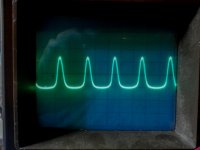
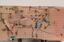
Hi , I tried this preamp with 2sa1837 mods on veroboard but this is what I see on the scope: I remade it three times and always the same pictures.
Input signal it is 2V and lowering it doesn't change much. I set different bias on R15 from 80mA to 170mA.
Input signal it is 2V and lowering it doesn't change much. I set different bias on R15 from 80mA to 170mA.
Attachments
Hi , I tried this preamp with 2sa1837 mods on veroboard but this is what I see on the scope: I remade it three times and always the same pictures.
Input signal it is 2V and lowering it doesn't change much. I set different bias on R15 from 80mA to 170mA.
As you made your own circuit I cannot say that you positively wired it correctly. Can you show schematic of your actual circuit with parts and values used? Also a good closeup photo of both sides of board. What is bias current through the LTP? What is your Vcc? What you show appears to be asymmetric behavior that may be caused by an issue in the Aksa Lender front end. Is the diode the correct type (1n4148 not Zener). Do you have transistor orientations correct for EBC and ECB depending on type?
Usually if bias in output exists the amp works - so something off in LTP.
Finally got the KSAs and popped them in today. However, I still have serious problems. The gain seems even lower than with the 2SA1837s, AND there is a terrible noise (hiss) on both channels. My build is pretty standard currently, with Q4 = KSA1381, all resistors according to the schematic except R11 = 2k2, for lower gain. With Vcc = 48V I measure the bias at 32.13mA and 31.63mA across R15 – not sure if this is correct.
Help – I don’t really know where to start looking for the error. I don’t even know what I should take photos of? Any pointers will be appreciated, thanks.
Help – I don’t really know where to start looking for the error. I don’t even know what I should take photos of? Any pointers will be appreciated, thanks.
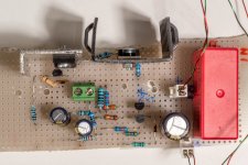
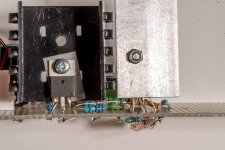
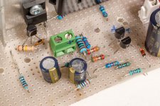
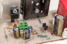
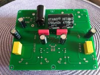
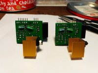
Then some photos of the protoboard.
Attachments
-
 aksa02509-08-2018.jpg205.8 KB · Views: 86
 -
 aksa02409-08-2018.jpg174.1 KB · Views: 106
 -
 aksa02309-08-2018.jpg339.5 KB · Views: 102
 -
 aksa02209-08-2018.jpg207.6 KB · Views: 96
 -
 aksa02109-08-2018.jpg219.2 KB · Views: 353
 -
 aksa01909-08-2018.jpg213.3 KB · Views: 353
 -
 aksa01809-08-2018.jpg203.9 KB · Views: 373
@twocents
Could you post fotos from equipped top PCB?
I had same problem and had do mistake with two populated resistors.
JP
Awesome - thank you very much JP for also making mistakes - I now found the problem with mine! I tried to take some photos but cannot get clear photos with my cell phone camera and artificial light. I then checked the orientation of the resistors against X's stuffing guide, and whala - there it is - R3 and R4A are incorrectly orientated. But to fix this will require some delicate soldering surgery. Damn, second mistake on this build.
But to fix this will require some delicate soldering surgery.
Contrary to popular belief, desoldering is not delicate but actually sloppy and messy... add lots of extra solder to the pads you want to remove to enhance the heat capacity to get it to soften to liquidus on both legs. When hot enough, pull out the offending part. Use solder sucker or copper braid with flux to clean up excess. Trick is not to pull on part until it is really liquid or a pad will come off too.
Thank you X for the de-soldering tips. It's waiting time again for me since I don't have those resistor values in my parts bin. I my case the resistors were not the offending parts - it was the offending builder who did not consult the documentation properly!
Wow, this is promising and worth the wait.... and now listing never ends.
JP
Hi everyone,
I am about to buy the PCBs kit to build this preamp. Will the PCB still contain errors (I have read earlier threads and saw some comments about a resistor and a diode I think)
or these were rectified in later revision PCBS (if there were any)?
Also, can someone tell me if this preamp is suitable to feed a valve amplifier? If so, should I isolate the preamp from the amp circuitry if I want to enclose this preamp IN the actual amp case? Aluminium case any good? Thanks a lot.
Errata - Please Read
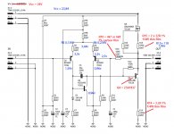
The PCBs themselves are fine, there was a typo on the schematic which had the V141 diode for the cap multiplier portion of the main board spec'd as a zener but it should just be a standard 1N400x or even a 1N4148 can work - it is a protection diode to protect the gate on the MOSFET.
These were noted in the main GB thread. Please consult Post 1 of this thread for updates to any errors.
As far as I know these are the only 3 errors or typos. A PCB error would actually mean that a trace was wired badly or missing.
1. Error on main PCB schematic: R141 Should be 10k not 220R.
2. Error on main PCB schematic: diode V141 should be standard 1N400X not breakdown or zener.
3. Revised BOM for MB (8-pin connector was incorrect), file here:
http://www.diyaudio.com/forums/attac...04_01_2018-zip
4. Error on SMT Daughterboard schematic: R102/103 were swapped, schematic updated now.
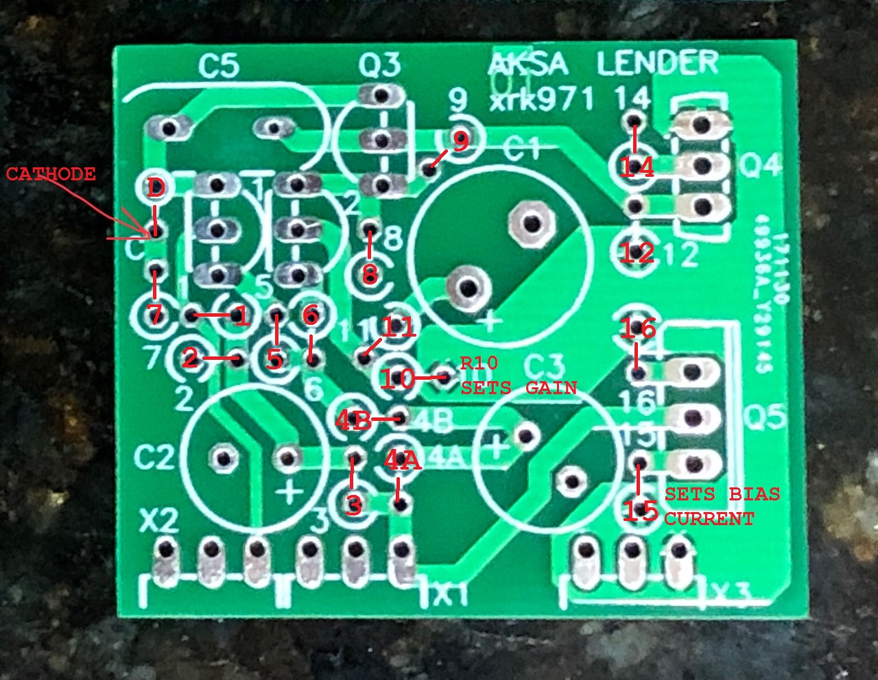
Here is the TH board stuffing guide - follow it exactly for pin placement:
The PCBs themselves are fine, there was a typo on the schematic which had the V141 diode for the cap multiplier portion of the main board spec'd as a zener but it should just be a standard 1N400x or even a 1N4148 can work - it is a protection diode to protect the gate on the MOSFET.
These were noted in the main GB thread. Please consult Post 1 of this thread for updates to any errors.
As far as I know these are the only 3 errors or typos. A PCB error would actually mean that a trace was wired badly or missing.
1. Error on main PCB schematic: R141 Should be 10k not 220R.
2. Error on main PCB schematic: diode V141 should be standard 1N400X not breakdown or zener.
3. Revised BOM for MB (8-pin connector was incorrect), file here:
http://www.diyaudio.com/forums/attac...04_01_2018-zip
4. Error on SMT Daughterboard schematic: R102/103 were swapped, schematic updated now.
Here is the TH board stuffing guide - follow it exactly for pin placement:
Last edited:
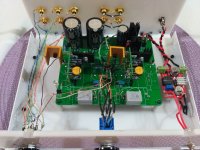
I finally got my Lender working! After some sloppy solder surgery the implants were successful – resistors R3 and R4A replaced, this time on the back of the boards. The rebellious twin daughters are doing what they are supposed to do now. The mother is no longer shorting and causing smoke in the house and the father provides clean power. My Lender family is happy and singing  . Almost filed for divorce a month ago.
The only mod on my build is R11 = 2k2. With this mod I feel the gain is still a bit low for my 88dB speakers. Only a quick listening test was done using a TDA7297 amp and Tannoy monitors. Maybe I must try something like 1k8 for R11? But this operation might be even more daunting as R11 is in the middle of the board. Anyway, I will test the Lender first with the ACA which I built it for.
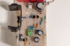
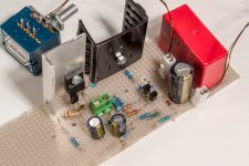
Many of the motherboard caps were mounted underneath the board. This was to make space for larger heatsinks on the daughter boards.
How does it sound? I only did a few quick songs using the TDA. Compared to the B1 the most notable differences are an increased soundstage and an enormous amount of bass! Really looking forward to connect the Lender to the ACA.
. Almost filed for divorce a month ago.The only mod on my build is R11 = 2k2. With this mod I feel the gain is still a bit low for my 88dB speakers. Only a quick listening test was done using a TDA7297 amp and Tannoy monitors. Maybe I must try something like 1k8 for R11? But this operation might be even more daunting as R11 is in the middle of the board. Anyway, I will test the Lender first with the ACA which I built it for.
Many of the motherboard caps were mounted underneath the board. This was to make space for larger heatsinks on the daughter boards.
How does it sound? I only did a few quick songs using the TDA. Compared to the B1 the most notable differences are an increased soundstage and an enormous amount of bass! Really looking forward to connect the Lender to the ACA.
Attachments

Nope - still something seriously wrong with my Lender. Need help (again) please. I found it simple and easy to solder another 2k2 resistor on the back of the pcb to the existing 2k2 R11 resistor, which brings the R11 value to 1k1 - pretty close to the standard 1k0 for full gain. However, the Lender signal is still very very soft. My B1 plays twice as loud, which means the Lender does not seem to be working at all. I measure bias values of 31.9mA and 31.7mA. This just does not look right to me.
So, all components are according to the schematic. I have gone over all the components – checked their values and orientation. I have checked all the solder joints. I am really not sure what to do next?
So, all components are according to the schematic. I have gone over all the components – checked their values and orientation. I have checked all the solder joints. I am really not sure what to do next?
Attachments
- Home
- Source & Line
- Analog Line Level
- AKSA's Lender Preamp with 40Vpp Output