A litte over 3 years ago I designed this :
http://www.diyaudio.com/forums/analog-line-level/254818-pop-click-free-hw-based-relay-attenuator.html
Now I can can finally release V2.")
Description :
Fully HW-based pop and click free relay attenuator.
All done with some clever use of digital logic and accurate timing.
127 x 0.6dB steps for an attenuation range of 0 to -76.2dB.
High quality Omron G6K relays, high quality low noise, low distortion 0.1% Panasonic 1206 ERA Thin Film resistors.
Perfect channel balance, from max to min attenuation.
The attenuator needs a 10K termination resistor to maintain a 10K total attenuator impedance.
Use a 100K Linear potentiometer to adjust the ADC input voltage.
150mm x 40mm 4 Layer ENIG PCB.
Changes from V1 :
1. Stepsize went from 0.65dB to 0.6dB.
2. Better stability. On V1 I tried to implement something that would stop the relays from changing state if the input voltage for the ADC was in the middle of 2 steps since it could lead to constant chatter of the relays. However it was not really as succesfull as I hope. This has now been fixed, been using the attenuator daily for more than a month and stability is 100%, not once has it started to chatter on its own, success.
3. Changed from Susumu RG 0.1% 0805 Thin Film resistors to Panasonic ERA 0.1% 1206 Thin Film Resistors.
4. Added onboard regulation for the Relays. Can be either 5VDC or 12VDC, depending on the supply voltage for the PCB.
5. PCB size increased to 150mm x 40mm to accomodate onboard supply for the relays.
6. PCB surface is now ENIG instead of HASL.
Attached is Digital Logic schematic, Supply-Relay schematic, component placement, BOM, Mouser BOM for 5VDC relays, Mouser BOM for 12VDC relays, Digikey BOM for 4 resistor values not available at Mouser, Picture of assembled PCB, closeup picture of a small modification that has to be performed for the board to work properly.
IMPORTANT - Read about the 2 necessary board modifications below - IMPORTANT
Modification 1:
Q2 Pin 8 and Pin 9 should not be soldered to their pads. Instead Pin 8 should be lifted and connected to GND pad of C16. Pin 9 should be lifted and connected to K1 Pin 1(either 5VDC or 12VDC depending on the supply voltage chosen for the relays).
Modification 2:
As you might have seen, JensH brought to my attention an issue with the clock input for U9. I have connected Pin 4 of U1 to Pin 1 on U9, it should have been U1 Pin 19 connected to U9 Pin 1. It does work with the wrong connection but there is a chance that it might not work.
The solution is to cut the track to U9 Pin 1 and connect a small wire from U1 Pin 19 to U9 Pin 1. Problem solved.
Build Tips :
1. Selecting relay voltage : If you supply the board with 7-14VDC order the 5VDC Mouser BOM with 5 VDC relays and 5VDC regulator. If you supply the board with 14-18VDC select the 12VDC Mouser BOM with 12VDC relays and 12VDC regulator. Common for both options is that you also need the Digikey BOM.
2. Selecting Potentiometer : Almost any 100K Linear potentiometer will work, but I personally use this one from Bourns :
Mouser : http://www.mouser.dk/ProductDetail/Bourns/53RAA-R25-A20L/?qs=sGAEpiMZZMs%252bPnt8BXTeX8gZvvuGLwav
Digikey : https://www.digikey.dk/product-detail/en/bourns-inc/53RAA-R25-A20L/53RAA-R25-A20L-ND/2564529
Ordering: Last time the price was 20$ per PCB for the V1 PCB. Now, even though the V2 PCB is bigger and has a more expensice ENIG surface finish I was once again going to set the price at 20$ per PCB. However, since I made a small error and the PCB requires a small modification for it to work the price is set at 15$ per PCB. The next batch, if there is enough interest, will be V3 with this small error fixed and price will be 20$ per PCB.
Shipping is 4$ anywhere in the world. Additional shipping charges may apply if the number of PCB's ordered exceed the weight limit for 4$ shipping.
Send me an E-mail with your DiyA username, real name and adress and I will send you a PayPal request. Since this is a hobby it might take me a day or two to reply and a few more days to ship. I hope people can live with that.
http://www.diyaudio.com/forums/analog-line-level/254818-pop-click-free-hw-based-relay-attenuator.html
Now I can can finally release V2.
Description :
Fully HW-based pop and click free relay attenuator.
All done with some clever use of digital logic and accurate timing.
127 x 0.6dB steps for an attenuation range of 0 to -76.2dB.
High quality Omron G6K relays, high quality low noise, low distortion 0.1% Panasonic 1206 ERA Thin Film resistors.
Perfect channel balance, from max to min attenuation.
The attenuator needs a 10K termination resistor to maintain a 10K total attenuator impedance.
Use a 100K Linear potentiometer to adjust the ADC input voltage.
150mm x 40mm 4 Layer ENIG PCB.
Changes from V1 :
1. Stepsize went from 0.65dB to 0.6dB.
2. Better stability. On V1 I tried to implement something that would stop the relays from changing state if the input voltage for the ADC was in the middle of 2 steps since it could lead to constant chatter of the relays. However it was not really as succesfull as I hope. This has now been fixed, been using the attenuator daily for more than a month and stability is 100%, not once has it started to chatter on its own, success.
3. Changed from Susumu RG 0.1% 0805 Thin Film resistors to Panasonic ERA 0.1% 1206 Thin Film Resistors.
4. Added onboard regulation for the Relays. Can be either 5VDC or 12VDC, depending on the supply voltage for the PCB.
5. PCB size increased to 150mm x 40mm to accomodate onboard supply for the relays.
6. PCB surface is now ENIG instead of HASL.
Attached is Digital Logic schematic, Supply-Relay schematic, component placement, BOM, Mouser BOM for 5VDC relays, Mouser BOM for 12VDC relays, Digikey BOM for 4 resistor values not available at Mouser, Picture of assembled PCB, closeup picture of a small modification that has to be performed for the board to work properly.
IMPORTANT - Read about the 2 necessary board modifications below - IMPORTANT
Modification 1:
Q2 Pin 8 and Pin 9 should not be soldered to their pads. Instead Pin 8 should be lifted and connected to GND pad of C16. Pin 9 should be lifted and connected to K1 Pin 1(either 5VDC or 12VDC depending on the supply voltage chosen for the relays).
Modification 2:
As you might have seen, JensH brought to my attention an issue with the clock input for U9. I have connected Pin 4 of U1 to Pin 1 on U9, it should have been U1 Pin 19 connected to U9 Pin 1. It does work with the wrong connection but there is a chance that it might not work.
The solution is to cut the track to U9 Pin 1 and connect a small wire from U1 Pin 19 to U9 Pin 1. Problem solved.
Build Tips :
1. Selecting relay voltage : If you supply the board with 7-14VDC order the 5VDC Mouser BOM with 5 VDC relays and 5VDC regulator. If you supply the board with 14-18VDC select the 12VDC Mouser BOM with 12VDC relays and 12VDC regulator. Common for both options is that you also need the Digikey BOM.
2. Selecting Potentiometer : Almost any 100K Linear potentiometer will work, but I personally use this one from Bourns :
Mouser : http://www.mouser.dk/ProductDetail/Bourns/53RAA-R25-A20L/?qs=sGAEpiMZZMs%252bPnt8BXTeX8gZvvuGLwav
Digikey : https://www.digikey.dk/product-detail/en/bourns-inc/53RAA-R25-A20L/53RAA-R25-A20L-ND/2564529
Ordering: Last time the price was 20$ per PCB for the V1 PCB. Now, even though the V2 PCB is bigger and has a more expensice ENIG surface finish I was once again going to set the price at 20$ per PCB. However, since I made a small error and the PCB requires a small modification for it to work the price is set at 15$ per PCB. The next batch, if there is enough interest, will be V3 with this small error fixed and price will be 20$ per PCB.
Shipping is 4$ anywhere in the world. Additional shipping charges may apply if the number of PCB's ordered exceed the weight limit for 4$ shipping.
Send me an E-mail with your DiyA username, real name and adress and I will send you a PayPal request. Since this is a hobby it might take me a day or two to reply and a few more days to ship. I hope people can live with that.
Attachments
-
Relay Attenuator V2B_Schematic_Digital Logic.pdf29.3 KB · Views: 400
-
Relay Attenuator V2B_Schematic_Supply-Relays.pdf27.7 KB · Views: 276
-
Relay Attenuator V2B_Component Placement.pdf26.2 KB · Views: 165
-
Relay Attenuator V2B_ BOM_Simple.pdf31.3 KB · Views: 134
-
Relay Attenuator V2_BOM_Mouser_Partial_5VDC.txt759 bytes · Views: 82
-
Relay Attenuator V2_BOM_Mouser_Partial_12VDC.txt760 bytes · Views: 73
-
Relay Attenuator V2_BOM_Digikey_Partial.txt65 bytes · Views: 75
-
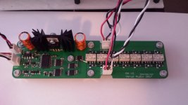 Boardfull.jpg424.4 KB · Views: 943
 -
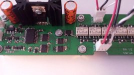 Closeup.jpg463.8 KB · Views: 928
Last edited:
are you using the voltage from this pot to adjust the volumes set by the relays?Use a 100K Linear potentiometer to adjust the ADC input voltage.
are you using the voltage from this pot to adjust the volumes set by the relays?
Yes, I am.
Do you have any extra boards for sale?
Yes, I do. I'll update my first post.
Hi Neutrality,
I've been looking for a similar solution using ADC0804 for a small headphone amp volume control. I have a question regarding the use of flip-flops after the ADC to control the relays. Why didn't you use the raw output of the ADC? I naively thought that if extreme values of the input voltage (over- or underflow) are avoided it should work or am I missing something?
Regards,
Oleg
Last edited:
Looks good
A few of suggestions:
1. Is U10 necessary? Couldn't you just scale the resistors R32 and R33 by e.g. a factor of 10 - 100? With a factor of 10 you would have a resistor to GND1 of 100 ohm, which is probably insignificant compared to the 100k potentiometer.
2. Wouldn't it be better to clock U9 from CLKR of U1? The signal swing at CLKIN may only be from 2.1 to 2.7V, worst case. I assume that CLKR is actually a square wave output, despite the fact that it is called an input in the pin list. At least the block diagram shows it as an output from an inverter. Whether the logíc high goes to the supply, I don't know. You should probably check, unless you have already done so.
3. I would suggest to put e.g. a 1k resistor in series with the base of Q1 or C5 to reduce the peak base current in Q1. You might be saved by the current limiter of the voltage regulator though.
Hi Neutrality,
I've been looking for a similar solution using ADC0804 for a small headphone amp volume control. I have a question regarding the use of flip-flops after the ADC to control the relays. Why didn't you use the raw output of the ADC? I naively thought that if extreme values of the input voltage (over- or underflow) are avoided it should work or am I missing something?
Regards,
Oleg
Simple really. If you were to control the realys without the Flip-flops you might risk having no attenuation at times when changing volume. Remember, when the realys are not turned on you have maximum attenuation, so when you turn up the volume you turn relays on and some off, but when you reach full volume, no attenuation, all relays are on. The problem is that realys do not make or break instantly, as an example, the realys I used has a make or break time of 3ms max, but it could be anywhere between ~1.5-3ms according to the datasheet.
Worst case is going from 1000000 to 0111111 where you might risk turning on all the LSB relays before you turn the MSB relay off. Basically you could risk it going from 1000000 to an intermediate value of 1111111 before you end up at your desired value of 0111111. 1111111 would be the same as no attenuation at all, not good.
By using 2 x octal flip-flops with their outputs fed into quad dual input and gates you can now control when the relays turn on and off.
Using the same example as above, you will now go from 1000000 to an intermediate value of 0000000 and end up at the final value of 0111111. Here 0000000 being full attenuation.
It is all about timing, you first take the realys that need to be turned off and turn them off and then 5ms after you turn on the relays that needs to be turned on. A full cycle take 10ms.
Hope that answers your question.
Looks good
A few of suggestions:
1. Is U10 necessary? Couldn't you just scale the resistors R32 and R33 by e.g. a factor of 10 - 100? With a factor of 10 you would have a resistor to GND1 of 100 ohm, which is probably insignificant compared to the 100k potentiometer.
2. Wouldn't it be better to clock U9 from CLKR of U1? The signal swing at CLKIN may only be from 2.1 to 2.7V, worst case. I assume that CLKR is actually a square wave output, despite the fact that it is called an input in the pin list. At least the block diagram shows it as an output from an inverter. Whether the logíc high goes to the supply, I don't know. You should probably check, unless you have already done so.
3. I would suggest to put e.g. a 1k resistor in series with the base of Q1 or C5 to reduce the peak base current in Q1. You might be saved by the current limiter of the voltage regulator though.
1. You are right, I could do without U10 if I scaled down the resistors R32 and R33. It could work, but the other way works as well, although I could save an opamp and a capacitor.
2. You are right. I just checked the CLKR and the CLKIN signals. CLKR is 0-5V square wave. CLKIN swings between 1.9-3.1V. Weird, I used CLKR on V1 but for some reason I used CLKIN on V2. However, the CLKIN signal feeds into U9 and the output from that is a perfect squarewave.
3. I havent really given it much thought, it worked fine in V1 and works fine in V2 but you might have a point. However, it is mostly an issue at turn on of the ADC, after that it is a non issue.
Thanks for the feedback.
I don't know if I will be doing anything about point 1, however point 2 and 3, especially 2 might be changed in V3.
Last edited:
I like the way you "detend" the pot with the LSB from the ADC. Neat, and a smart design overall. Have been thinking about doing the relay control with an Arduino lately, but your hard-wired logic control seems to be more straight forward. Thanks for sharing.
My little question is, would it be possible to do it with a two layer PCB instead of a four-layer one, without compromising performance?
My little question is, would it be possible to do it with a two layer PCB instead of a four-layer one, without compromising performance?
........
3. I havent really given it much thought, it worked fine in V1 and works fine in V2 but you might have a point. However, it is mostly an issue at turn on of the ADC, after that it is a non issue.
....An alternative might be to replace Q1 with a MOSFET, BSS138 alike , to eliminate the current surge at power on. C5 could then be sized down a lot as well.
....An alternative might be to replace Q1 with a MOSFET, BSS138 alike , to eliminate the current surge at power on. C5 could then be sized down a lot as well.
Or a 2n7002, I use those for many other things and have a few at hand.
I like the way you "detend" the pot with the LSB from the ADC. Neat, and a smart design overall. Have been thinking about doing the relay control with an Arduino lately, but your hard-wired logic control seems to be more straight forward. Thanks for sharing.
My little question is, would it be possible to do it with a two layer PCB instead of a four-layer one, without compromising performance?
Thanks, it took me a while to find a solution that would keep the circuit stable at all times, I have considered many options and none turned out well when I really looked at them , except this solution.
As for your question, yes it could be done on a 2-layer PCB's, but since 4-Layer PCB's have come significantly down in price the last few years I usually just go for 4-Layer.
Overkill, yes, but makes things a lot easier and simple to layout.
As you might have seen, JensH brought to my attention an issue with the clock input for U9. I have connected Pin 4 of U1 to Pin 1 on U9, it should have been U1 Pin 19 connected to U9 Pin 1. It does work with the wrong connection but there is a chance that it might not work.
The solution is to cut the track to U9 Pin 1 and connect a small wire from U1 Pin 19 to U9 Pin 1. Problem solved.
The funny thing is, that it was connected correctly on V1, the same goes for Q2 Pin 8 and Pin 9 which were connected correctly on V1.
But from V1 to V2 I redid all my components, better schematic symbols, better footprints, manufacturer part number, supplier part number etc. Then when redoing the schematic those 2 errors crept in.
Now sdince this is 2 modifications to the board, I think it is fair if thsoe who have ordered PCB's to get a chance to reconsider.
So for thsoe whoe have ordered PCB's, if you still want them or not send me a message and let me know. I understand if you have second thoughts. That is the only fair way to deal with it.
I will not be sending any payment requests until people have messaged me.
The first post is updated with the new modification.
The solution is to cut the track to U9 Pin 1 and connect a small wire from U1 Pin 19 to U9 Pin 1. Problem solved.
The funny thing is, that it was connected correctly on V1, the same goes for Q2 Pin 8 and Pin 9 which were connected correctly on V1.
But from V1 to V2 I redid all my components, better schematic symbols, better footprints, manufacturer part number, supplier part number etc. Then when redoing the schematic those 2 errors crept in.
Now sdince this is 2 modifications to the board, I think it is fair if thsoe who have ordered PCB's to get a chance to reconsider.
So for thsoe whoe have ordered PCB's, if you still want them or not send me a message and let me know. I understand if you have second thoughts.
That is the only fair way to deal with it.I will not be sending any payment requests until people have messaged me.
The first post is updated with the new modification.
Last edited:
Is one (1) PCB required for a stereo attenuator?
Can multiple PCBs be used to control multiple channels and keep them all level aligned? eg 3PCBs for a 5.1 system, or the 6 outputs from a DCX24/96
Yes, 1 PCB for a stereo attenuator and no, you cant really use multiple PCB's if you want to keep them level aligned.
- Status
- This old topic is closed. If you want to reopen this topic, contact a moderator using the "Report Post" button.
- Home
- Source & Line
- Analog Line Level
- Pop/click free HW-based relay attenuator V2