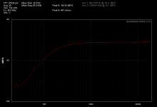
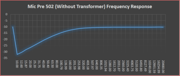
I've been working on this mic preamp, doing some repairs and light mods, and I can't for the life of me figure out why there is this rolloff happening at around 120 Hz (see frequency response graph attached).
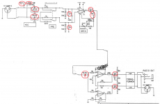
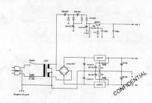
If you look at the schematics (see below), it is basically a generic SSM2019-based mic pre with a cross-coupled floating differential output stage.
I'm using 1.2k bias resistors on the SSM2019 inputs, and I thought maybe the low-ish input resistance after the 100uF phantom blocking caps could be the culprit, but it doesn't add up because the -3 dB rolloff should be around 1.5 Hz.
Just for my own sanity I've checked that it's not my QA400 or the balanced to unbalanced input/output converter (THAT 1206 & 1246) that I'm using.
I've circled in red all parts of the schematic that I've thought could possibly be related to this. I've also attached the original schematic (without mods), just for reference.
Any thoughts?
Attachments
Hi CZ
I would think that it is the output transformer. Measure @ the output of each stage to verify and complete the debug process.
Duke.")
Good observation, however as is there's no output transformer installed. The output is just straight off of C5 and C6.
Which of the suspect electrolytics have you replaced already?
Are you aware that your 1k2 bias resistors are doing input CMRR no favors? I don't see the point of this change. The original 2k resistor in the pad would not have done this. If you do want to reduce DM input impedance, use a T arrangement, which allows keeping CM input impedance high - like 4k7 + 4k7, midpoint going to ground via 10-22k. No reason to overdo it either, in the end your limit will be the 6k8 P48V bias resistors. Right now you're wasting about 16 dB of CMRR though.
Input filtering can be carried out in a similar way.
Also inspect XLR pin 1 routing - in accordance with AES48-2005 this should go to chassis first (on as short and direct a path as possible), which then connects to circuit ground elsewhere.
Last edited:
Which of the suspect electrolytics have you replaced already?
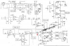
All of them. Also, I doubled all signal path electrolytic caps' size except for the phantom blocking caps. The reason I didn't increase the phantom blocking caps' size is because I didn't want to overstress the SSM2019's input protection diodes. I actually removed those 5V6 diodes from before the SSM2019's input but I forgot to reflect that on the schematic. I've attached an updated schematic that shows more accurately what was done.
Are you aware that your 1k2 bias resistors are doing input CMRR no favors? I don't see the point of this change. The original 2k resistor in the pad would not have done this. If you do want to reduce DM input impedance, use a T arrangement, which allows keeping CM input impedance high - like 4k7 + 4k7, midpoint going to ground via 10-22k. No reason to overdo it either, in the end your limit will be the 6k8 P48V bias resistors. Right now you're wasting about 16 dB of CMRR though.
Thanks. No I was not aware of this as I'm kind of ignorant in this area, unfortunately. My overall goal here was to reduce noise and improve CMRR, but I guess I failed - at least in the latter case. I did match the 1.2k resistors as closely as I could with my LCR meter - to better than .1%.
It was my understanding that using a resistor across the +/- inputs (like the 2k in the original schematic) is a way to achieve a tighter tolerance between the two bias resistors - by reducing whatever ratio of mismatch there may be between them. Are there any other reasons, engineering-wise, that the 2k across the +/- inputs could lead to improved CMRR?
Also, I've read about the T config being better for CMRR, although I have to admit I do not completely understand why or how. I remember reading that the T config presents a "higher common mode impedance to ground"? I imagine this as a common mode signal having nowhere to go but through the single resistor to ground - and so the differentially connected resistors in the T network each convert common mode to diff mode by their fractional relationship with the middle resistor as common denominator - rather than by the full mismatch ratio of the two bias resistors? Sorry if this makes no sense. Any light you have to shed on this would be greatly appreciated.
Input filtering can be carried out in a similar way.
Also inspect XLR pin 1 routing - in accordance with AES48-2005 this should go to chassis first (on as short and direct a path as possible), which then connects to circuit ground elsewhere.
I had added some rf filtering caps directly at the input jack but I forgot to include them - see updated schematic.
Also, this pre did have the "pin 1 problem", so I re-routed the XLR shield directly to chassis.
Attachments
That's an extremely good point, well spotted. Obviously if something is hooked up wrong in the measurement setup, all bets are off and we may be chasing a red herring down a rabbit hole.
It may reduce noise if you have a noisy P48V supply to contend with, though in this case I'd rather clean that one up (what's it look like?).Thanks. No I was not aware of this as I'm kind of ignorant in this area, unfortunately. My overall goal here was to reduce noise and improve CMRR, but I guess I failed - at least in the latter case. I did match the 1.2k resistors as closely as I could with my LCR meter - to better than .1%.
Other than that your dominant noise source is going to be the mic pre or its source impedance.
That's technically true but doesn't help you in practice since you have reduced common-mode input impedance at the same time.It was my understanding that using a resistor across the +/- inputs (like the 2k in the original schematic) is a way to achieve a tighter tolerance between the two bias resistors - by reducing whatever ratio of mismatch there may be between them.
Where it would help CMRR would be in the input pad. The way that is done now, it attenuates differential mode but not common mode at all, so it really is just an overload fix that also worsens CMRR at the same time. I can't see a way of switching in both series and two parallel resistors to ground using just one DPDT switch though. I guess one could argue that by the time you need an input pad, you've got plenty of signal to begin with and worse CMRR is no biggie...
Speaking of pad, that I think is why they had the 2k resistor in there originally, so that differential input impedance would not vary too much between pad in/out (reducing pop/click noise when switching).
Any signal can be represented as a linear combination of two orthogonal components:Also, I've read about the T config being better for CMRR, although I have to admit I do not completely understand why or how. I remember reading that the T config presents a "higher common mode impedance to ground"?
1. Differential mode, which is symmetrical about ground - it's an out-of-phase excitation of your hot and cold lines.
2. Common mode, which is an in-phase excitation of hot and cold relative to ground.
Do you know mid-side stereo, where things are split into L+R and L-R components? Same idea.
To make a long story (recommended reading) short, while gain matching is still important, practical CMRR especially in the face of non-ideally-matched source impedances is often limited by common-mode input impedance, which should thus be as high as possible. It's great when your instrumentation amp IC with laser-trimmed resistors states 95 dB of CMRR, but that doesn't help when the components preceding it turn (unwanted) common mode into differential mode.
You now have to look into your circuit's input for both of these cases.
For differential mode, we are seeing:
* 2x 100p in series = 50p
* 2x 6k81 in series = 13k62
* input caps can be ignored at AC
* 1k2 + 1k2 = 2k4
* 220p
all in parallel. (I have assumed INA inputs to be just about open, which is a reasonably approximation.)
At low freqs, that's about
* 2x 6k81 in series = 13k62
* 1k2 + 1k2 = 2k4
Or about 2k04.
For common mode, we are basically tying both inputs together. That gives us:
* 2x 100p in parallel
* 2x 6k81 in parallel
* 2x 1k2 in parallel
At low freqs, that's about 510 ohms. Not my definition of "high" for sure!
Now let's look at what a T-type config looks like for both cases. Let's grab your 1k2s but run their midpoint to ground via a 10k.
In DM, you get 1k2 + 1k2 in series = 2k4.
In CM, you get 2x 1k2 in parallel, with 10k in series = 10k6.
(The CM case would have been just 600 ohms before, contributing the majority of the 510 ohms above.)
Total impedances with this in circuit would thus be:
In DM: 2k04 (unchanged)
In CM:
* 2x 6k81 in parallel with
* 10k6
which is ~= 2k58, more than 5 times as high as before and getting reasonably close to the theoretical maximum of 3k405.
Arguably 47p would also have done the job, but anyway.I had added some rf filtering caps directly at the input jack but I forgot to include them - see updated schematic.
Yeah - I don't know why the QA400 uses such a weak impulse chirp in its FR measurement mode. It might have something to do with avoiding clipping, and/or minimizing slew-induced TMD?
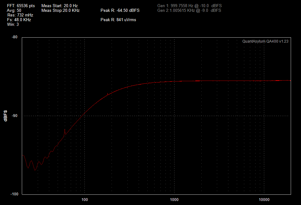
The QA400 does have the capability with an included "plug in" (basically a Python script) to perform a frequency response measurement over a wider dynamic range. The thing is it exports this data as a .csv file and then you have to plot it somehow if you want a graph. I tried to create a plot in Excel but I gave up after a while (I'm not so keen on Excel). Anyway, the "plug in" measurement results corroborate the QA400's weak impulse FR measurements (see attached).
Attachments
Mmkay. Still, would you mind describing your measurement setup's wiring in detail, just in case?
The only way the amp could be at fault now would be some sort of bad ground connection or other intermittency, maybe a lifted pad or cracked PCB somewhere. Make sure you're getting good continuity from every supposedly "grounded" node to star ground / transformer center tap / chassis, as well as supposedly connected points along the signal path.
The only way the amp could be at fault now would be some sort of bad ground connection or other intermittency, maybe a lifted pad or cracked PCB somewhere. Make sure you're getting good continuity from every supposedly "grounded" node to star ground / transformer center tap / chassis, as well as supposedly connected points along the signal path.
That's an extremely good point, well spotted. Obviously if something is hooked up wrong in the measurement setup, all bets are off and we may be chasing a red herring down a rabbit hole.
It may reduce noise if you have a noisy P48V supply to contend with, though in this case I'd rather clean that one up (what's it look like?).
It's a fairly typical voltage tripler followed by a single wave rectifier and a zener-based single BJT regulator with some negative feedback between collector and base (see schematic attached). I replaced all caps with new electrolytics and the 100pF caps with NP0.
I did a scope check for ripple and noise and it was pretty low (1 mV PP), although I didn't test it under load. I should try that the next time I have it open.
Where it would help CMRR would be in the input pad. The way that is done now, it attenuates differential mode but not common mode at all, so it really is just an overload fix that also worsens CMRR at the same time. I can't see a way of switching in both series and two parallel resistors to ground using just one DPDT switch though. I guess one could argue that by the time you need an input pad, you've got plenty of signal to begin with and worse CMRR is no biggie...
Speaking of pad, that I think is why they had the 2k resistor in there originally, so that differential input impedance would not vary too much between pad in/out (reducing pop/click noise when switching).
Any signal can be represented as a linear combination of two orthogonal components:
1. Differential mode, which is symmetrical about ground - it's an out-of-phase excitation of your hot and cold lines.
2. Common mode, which is an in-phase excitation of hot and cold relative to ground.
Do you know mid-side stereo, where things are split into L+R and L-R components? Same idea.
To make a long story (recommended reading) short, while gain matching is still important, practical CMRR especially in the face of non-ideally-matched source impedances is often limited by common-mode input impedance, which should thus be as high as possible. It's great when your instrumentation amp IC with laser-trimmed resistors states 95 dB of CMRR, but that doesn't help when the components preceding it turn (unwanted) common mode into differential mode.
You now have to look into your circuit's input for both of these cases.
For differential mode, we are seeing:
* 2x 100p in series = 50p
* 2x 6k81 in series = 13k62
* input caps can be ignored at AC
* 1k2 + 1k2 = 2k4
* 220p
all in parallel. (I have assumed INA inputs to be just about open, which is a reasonably approximation.)
At low freqs, that's about
* 2x 6k81 in series = 13k62
* 1k2 + 1k2 = 2k4
Or about 2k04.
For common mode, we are basically tying both inputs together. That gives us:
* 2x 100p in parallel
* 2x 6k81 in parallel
* 2x 1k2 in parallel
At low freqs, that's about 510 ohms. Not my definition of "high" for sure!
Now let's look at what a T-type config looks like for both cases. Let's grab your 1k2s but run their midpoint to ground via a 10k.
In DM, you get 1k2 + 1k2 in series = 2k4.
In CM, you get 2x 1k2 in parallel, with 10k in series = 10k6.
(The CM case would have been just 600 ohms before, contributing the majority of the 510 ohms above.)
Total impedances with this in circuit would thus be:
In DM: 2k04 (unchanged)
In CM:
* 2x 6k81 in parallel with
* 10k6
which is ~= 2k58, more than 5 times as high as before and getting reasonably close to the theoretical maximum of 3k405.
Thanks for the great explanation. It's coming into focus a bit more - the idea that high common mode input impedance is desirable so as to create a low-ratio voltage divider minimizing the imbalances in the preceding low output impedance driver stage as they get converted to diff mode. Please correct me if this is wrong!
Attachments
Mmkay. Still, would you mind describing your measurement setup's wiring in detail, just in case?
The only way the amp could be at fault now would be some sort of bad ground connection or other intermittency, maybe a lifted pad or cracked PCB somewhere. Make sure you're getting good continuity from every supposedly "grounded" node to star ground / transformer center tap / chassis, as well as supposedly connected points along the signal path.
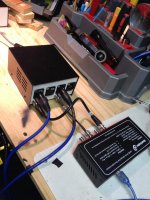
In the attached pic, imagine that the pre is connected in/out with the blue XLR cables going from and coming to the white box.
Inside the white box is a THAT 1246 driver stage and a THAT 1206 input stage, both connected via BNC to the QA400's output and input, respectively.
Attachments
Are you sure the rolloff is not deliberate to mitigate the proximity effect?
Well, if it's intentional then there should be a physical explanation for it - and according to the schematic - to me at least it makes no sense why there would be this rolloff.
Like sgrossklass said it has to be something physically awry in the actual routing on the PCB or something wrong with a component, but I just can't figure out what it could possibly be, because I've checked and re-checked and it's same on two identical channels.
To answer your question, yes - it's not deliberate. The preamp has a switchable high-pass filter but I've checked and it's correctly out of circuit with the switch off (I thought for a bit that maybe this had been wired with the switch backwards, but actually it's wired correctly).
Okay, well just a thought. You apparently have ruled it out correctly.
100 pF? Erm, it says 100n in the schematic, and you'd be reasonably hard-pressed to obtain 100 nF NP0s rated for >50 V, so please double check. The type of these caps is not too critical, any decent films will be plenty.It's a fairly typical voltage tripler followed by a single wave rectifier and a zener-based single BJT regulator with some negative feedback between collector and base (see schematic attached). I replaced all caps with new electrolytics and the 100pF caps with NP0.
I wouldn't call that negative feedback at all, it's just a bias resistor - an emitter follower is an inherently almost 100% feedback circuit though. Also 100n for the zener sounds like a good joke, I'd try whacking in 100 µF in parallel to that. The stock 100n output cap sounds OK though, EFs aren't too fond of capacitive loading anyway. I guess they got away without a base stopper resistor because the BD237 is a pretty slow part (3 MHz fT nom @250 mA Ic). Certainly worth keeping an eye on any kind of oscillation.
Re: the +/-18 V supply:
Knowing LM317/337s, 22µ on the output seems a bit low. I'd up that to more like 220µ, adding the recommended protection diodes (2 per reg) while you're at it. Thanks to the ADJ pin cap, it's a low-noise design to begin with, which is nice.
Now if only you could find out where your invaluntary highpass is hiding out. Thorough inspection with a multimeter and magnifying glass may be needed here. I like using an old 28mm f/2.8 manual focus SLR lens in reverse for this, I have some floating around anyway and their extra backfocus distance (and optical quality) comes in handy.
100 pF? Erm, it says 100n in the schematic, and you'd be reasonably hard-pressed to obtain 100 nF NP0s rated for >50 V, so please double check. The type of these caps is not too critical, any decent films will be plenty.
My bad - 100nF they are.
I wouldn't call that negative feedback at all, it's just a bias resistor - an emitter follower is an inherently almost 100% feedback circuit though.
Thanks. That makes sense. I guess I was thinking that the DC voltage ripple after the single-wave rectifier would be compensated for somewhat by appearing at the base.
Also 100n for the zener sounds like a good joke, I'd try whacking in 100 µF in parallel to that. The stock 100n output cap sounds OK though, EFs aren't too fond of capacitive loading anyway. I guess they got away without a base stopper resistor because the BD237 is a pretty slow part (3 MHz fT nom @250 mA Ic). Certainly worth keeping an eye on any kind of oscillation.
Good idea.
Now if only you could find out where your invaluntary highpass is hiding out. Thorough inspection with a multimeter and magnifying glass may be needed here. I like using an old 28mm f/2.8 manual focus SLR lens in reverse for this, I have some floating around anyway and their extra backfocus distance (and optical quality) comes in handy.
I'm starting to think I need to cross check the measurement on another sound card, so I'm going to do that tomorrow and see.
Be careful with the levels you send into the input though, we are potentially talking mic level after all. Not sure the thing can get to unity gain even at minimum gain setting and pad enabled. Ideally I'd want to have an attenuator.
The QA400 uses a very weak signal in its freq response test mode - like around .8mV.
When I test a mic pre with the QA400 at its output relative to full scale (1.41Vrms), I use a string of four -6 dB BNC attenuators in series after the QA400's signal gen output set at around -20 dBFS. I can get down to about a 10 mV p-p signal this way, which is a good approximation for a microphone signal.
- Status
- This old topic is closed. If you want to reopen this topic, contact a moderator using the "Report Post" button.
- Home
- Source & Line
- Analog Line Level
- SSM2019 Mic Pre Lows Rolloff at 120 Hz - Why?