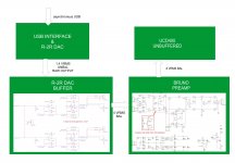
6 Preamp can accept single-ended input from resistor ladder DAC. Negative input is shorted to the ground.
Again, not to pick nits, but 'shorted to ground' is incorrect. The neg input is in this case the reference for the pos input, so it should be connected to the reference of the SE DAC output, which is the return or screen of the SE input cable. Definitely NOT ground!
Jan
and where did 625ohms output impedance come from?This information is here:
https://hifiduino.wordpress.com/2015/01/30/building-soekris-r-2r-dac/
The manufacturers often do not want to bother with unusual causes, especially when someone is not so much knowledgeable as me.
Someone should explain me patienly point-to point method what would be best and simplest way to connect DAC and amplifier with circuits available below. I have even made block diagram of my desired system...I will post it here but every further discussion regarding this issue should be directed to my PM in order to avoid rubbish in this thread. Thanks! I will read through all your answers throughly later in the day when I come back home.
You have a balanced impedance output. You have a balanced impedance input.
You have the information to adjust the gains to just hit maximum output at 0dBfs.
The only bit missing is a volume control. Or is that in the DAC?
You can use the B.Putzeys balanced volume control without any modifications. The Power Amp gain adjustment as in the Hypex document.
If you can't do that then get the manufacturer to alter for you, or supply the information to allow a competent repairer to do it for you.
Last edited:
and where did 625ohms output impedance come from?
You have a balanced impedance output. You have a balanced impedance input.
You have the information to adjust the gains to just hit maximum output at 0dBfs.
The only bit missing is a volume control. Or is that in the DAC?
You can use the B.Putzeys balanced volume control without any modifications. The Power Amp gain adjustment as in the Hypex document.
If you can't do that then get the manufacturer to alter for you, or supply the information to allow a competent repairer to do it for you.
DAC have volume control but it is better to have analog regulation as well, especially whet it is so "transparent" as Bruno's approach. I want to leave UCD modules intact.
There are 2 approaches left:
1) boost gain of DAC output buffer
2) boost gain of Bruno preamp buffer
I have no information which values to change in order to raise gain in the DAC buffer.
Instead of 1:1 buffer stage of preamplifier, LM4562 buffer from UCD datasheet can be used, but with gain lowered from 13dB to, say, 6dB in order to save resistors from excessive heat dissipation.
One of this two approaches may be good.
Attachments
and where did 625ohms output impedance come from?
??
It came from the spec sheet of the DAC he's using - and as it is the only mention of 625ohms on this thread, that must have been where you saw it too.
WindForce85 is not the designer of the DAC!
You are not interested in listening,
Due to your roundabout way of hiding and then revealing information, you have wasted all our time.
I am not interested in trying to guide you any further.
Go your own way.
You seem to be being rather grumpy and in your own world - as I read the questions asked, they are reasonable from a beginner's point of view and it is obvious from the start that he simply wants to see how/whether this volume control/preamp can be interfaced easily to the UCD400, bypassing the UCD's input buffer (and optimised with the DAC's output in mind).
Reading your replies it appears to me you are replying from a point of view which may be clear in your head but to anyone on the outside may be far from clear - as a beginner in this kind of thing too, I'm seeing things from WindForce85's point of view.
Effective communication is only as good as the weakest link so don't get all grumpy because you're not communicating with a beginner properly in beginner's terms.
I think you're being a bit too harsh.
(and don't speak for me by saying he's wasted "all OUR time" - not at all from my point of view. Thanks to WindForce85 for bringing up the topic!)
Last edited:
AndrewT said:You have a balanced impedance output. You have a balanced impedance input. You can use the B.Putzeys balanced volume control without any modifications
If you disable the balanced impedance output and use the unbalanced output, then you don't need a balanced input pre-amp.
Sorry but you should take into an account that I am a newbie. And I also cannot read in your mind as you cannot read in mine so why angry? It is good that I can tell apart opamp from preamp!That is what you should have asked in your first post. Instead of hiding all the information you had to hand !!!!!!!
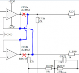
I didn't hide anything to spite you.I've been going over the circuit and the PCB and I think there is an inversion between hot and cold sides of the signal.
I know there's a potential group buy going on (I tentatively signed up for a bare board ) but I went ahead to trace this through and have spotted a few things which might have been inverted.
The schematic shows the "A" side of the LM4562 U1/U6 for the positive leg of the differential input and the "B" side as the negative leg. Taking the positive leg, this has output pin 1 which then goes to R30 and R34.
However, looking at the board and the traces, the "A" side of LM4562 goes to R40 and R43 (the negative leg). Inversely, the "B" side of LM4562 goes to R30 and R34...
This suggests that the TL072 side of the circuit which acts as a kind of DC filter is reversed (I haven't fully understood how that works, still analysing it ).
Following through the circuit, it then seems to follow the same "polarity" as in the schematic: the upper half is the positive side, the lower half the negative. On the output side, the positive leg goes to pin 2 of J2/J8 and the negative leg goes to pin 3. So it isn't inverted back.
Doesn't that mean that the outputs are out of phase with the inputs?
I know there's a potential group buy going on (I tentatively signed up for a bare board
) but I went ahead to trace this through and have spotted a few things which might have been inverted.The schematic shows the "A" side of the LM4562 U1/U6 for the positive leg of the differential input and the "B" side as the negative leg. Taking the positive leg, this has output pin 1 which then goes to R30 and R34.
However, looking at the board and the traces, the "A" side of LM4562 goes to R40 and R43 (the negative leg). Inversely, the "B" side of LM4562 goes to R30 and R34...
This suggests that the TL072 side of the circuit which acts as a kind of DC filter is reversed (I haven't fully understood how that works, still analysing it
).Following through the circuit, it then seems to follow the same "polarity" as in the schematic: the upper half is the positive side, the lower half the negative. On the output side, the positive leg goes to pin 2 of J2/J8 and the negative leg goes to pin 3. So it isn't inverted back.
Doesn't that mean that the outputs are out of phase with the inputs?
Attachments
Last edited:
Thanks Jan, that makes sense.
And the circuit to illustrate:
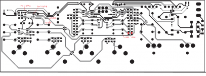
That's not a circuit. Trying to figure out a circuit from the PCB is asking for lots of headaches!
Remember that these PCB systems translate a schematic 1:1 into a layout, and raise an error if you deliberately want to make a different routing than the schematic wants. You may want to google PCB ERC and such.
If someone feels that the PCB is different than the schematic, it is very likely that they oversaw something. Not impossible, but extremely unlikely.
In my 20+ years of PCB layout I still haven't found a single case of a PCB being different than the schematic.
Jan
I forgot to prefix with printed and suffix with board - I meant PCB
I know what you mean, I understand ERC and PCB design (I'm learning KiCad now). My point is that putting aside an ERC error which, as you say, is incredibly unlikely, then the schematic and the PCB layout do differ, most likely from a different version or something. The PCB clearly shows pins 1/2 (the A part) of U6 going to R43 and pins 6/7 (the B part) going to R34. The electronic schematic has it the other way around
I wanted to "reverse engineer" it - and give myself some headaches in the process! - purely because Bruno put some really interesting ideas like the net ties / "electron dump" and I wanted to understand how it mapped from an electronic schematic which is the "theory" to the PCB which is the reality.
At first when I saw this, I thought that it must have just been the references put in the wrong place compared to the resistors for example, but following the actual tracks, they (tracks) are in line with the references which differ from the schematic.
I night very well be wrong of course, but having double and triple checked the mapping, if I'm not wrong, then either the design rule check was having a day off or some other discrepancy krept into the design
Regarding my post, please feel free to flick your avatar switch to the down position
Last edited:
I forgot to prefix with printed and suffix with board - I meant PCB
I have a spare board, I'll check it tomorrow.
The use of an ohmmeter suggests itself.
Jan
Why not
Do you see what I mean though between the PCB and the schematic?
Xavier
No I don't have it here, but by coincidence I have debugged one unit this afternoon and understand what you mean though.
Hi Jan, did you get the chance to look?
I have a spare board, I'll check it tomorrow.
The use of an ohmmeter suggests itself.
Jan
I forgot to prefix with printed and suffix with board - I meant PCB
I know what you mean, I understand ERC and PCB design (I'm learning KiCad now). My point is that putting aside an ERC error which, as you say, is incredibly unlikely, then the schematic and the PCB layout do differ, most likely from a different version or something. The PCB clearly shows pins 1/2 (the A part) of U6 going to R43 and pins 6/7 (the B part) going to R34. The electronic schematic has it the other way around
I wanted to "reverse engineer" it - and give myself some headaches in the process! - purely because Bruno put some really interesting ideas like the net ties / "electron dump" and I wanted to understand how it mapped from an electronic schematic which is the "theory" to the PCB which is the reality.
At first when I saw this, I thought that it must have just been the references put in the wrong place compared to the resistors for example, but following the actual tracks, they (tracks) are in line with the references which differ from the schematic.
I night very well be wrong of course, but having double and triple checked the mapping, if I'm not wrong, then either the design rule check was having a day off or some other discrepancy krept into the design
Regarding my post, please feel free to flick your avatar switch to the down position
I have just looked at my schematic (page 121 of Vol 5) and pin 1 & 2 of U6A (top left IC) are shown to go to R34, and pin 6 & 7 of U6B going to R43. Indeed on the PCB this is reversed, as measured for continuity.
Hmmm...
I'll ask Bruno what gives.
Jan
- Home
- Source & Line
- Analog Line Level
- BPPBP - Bruno Putzey's Purist Balanced Preamp (well a balanced volume control really)