Hi, keantoken.
Just a quick question about the new layout you are working on.
What is the purpose of the new PCB? To make it more applicable or will it improve the audible performance?
I have the board supplied from Dirt Cheap Dirty Boards. Will there be any improvements in your opinion to go with the new layout?
reg
The new PCB will be more functional, but sound quality won't be any different. The first one has some errors, and I've gotten a bit better at PCB layout since then. I'm nearly out of PCBs, so it's only natural to make some updates. In short, the PCB is changing because I'm changing.
Last edited:
Do that mean that there is some errors on the PCBs from DCDB?
Could you then please point me to the post where it is corrected?
Thanks!
I'm not sure what that is. But, here so far is the pertinent build information for the the first set of PCBs I designed:
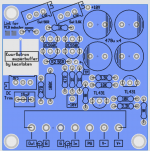
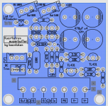
Important info for Kuartlotron PCBs!
1: The boards need a +-10V PSU, do not use more. For trimming you want a regulated supply, but you can still use a simple PSU if the ripple is under 20mV or so.
2: Each board is one channel, so you need a pair for stereo.
3: Some quick notes on construction:
a: Component values are shown on the PCB.
b: It accepts screw terminal inputs and outputs and M3 standoffs.
c: Transistors on left are BC560C (PNP), Transistors on right are BC550C (NPN). Heatshrink or glue the transistors face to face.
d: Use either an inductor, or bridge the solder link in the upper right to use the PCB inductor.
e: Set the trimmers to the values shown on the PCB before soldering them, or just use resistors of those values in the outer vias.
f: Place the screw on the trimmers over screw on the silkscreen. Otherwise the turning direction will be reversed.
4: Customizations:
a: Input resistance is normally 100k. You can use 10k if you want.
b: Output impedance is set to 47R for driving cables to reduce reflections. If you want lower output impedance you can use 4.7R in place of the 47R resistor.
Setup procedure:
1: Each trimmer should be set to the value indicated on the PCB. This can be done before soldering them.
2: Short the input and adjust R5 so that TP reads half of V+ (5V).
3: Remove short from the input and then adjust the DC trimmer so that input voltage reads 0.
Output offset should now be within 5mV. This generally results from small variances in components and won't reduce performance.
Errata:
The connection between the 270R and 15pF capacitor must be made off the PCB. Those vias are mistakenly grounded, which generally causes reduced volume and low input impedance. If you have already soldered the boards, you can clip the leads where they go into the board, lift them up and solder them back together above the board.
Sorry for the mistake. I did not discover the error because it did not cause any obvious faults.
Last edited:
My boards stack, so just add some standoffs, rather than drilling holes.
BOM
Here is the BOM. Some people want to use special resistors, so it has Vishay 1/8W metal film resistors which should fit on this PCB.
you should remove the .txt extension for the excel file. Opening the excel in notepad is a mess just in case if someone unaware !
DIYaudio won't accept .xls files.
About 16-17mA, can be more or less.
Looking through drawers to see what parts I can use for a power supply. What's the steady state current consumption of the circuit on the webpage? (Please forgive if already posted somewhere but I didn't see it.)
Thanks
About 16-17mA, can be more or less.
DIYaudio won't accept .xls files.
About 16-17mA, can be more or less.
does this means that using batteries is possible ?
Ah, I didn't now there was EMC problems with holes in a ground plane - doesn't apply to the component holes? Ideally, smd components only on the one layer?
Can bigger clearance holes, irregular shaped apertures, slotted/sectional planes (as per Tentlabs), etc reduce the EMC reasons or does any/all perforations create problems? [Is it a design protocol and how significant to sound quality would it be to ignore it?]
Circular holes are the most benign, so the pins aren't too bad. In most cases, perforations probably don't cause problems for audio unless there is a grounding mistake. But I figure, if it has a ground plane, why not go all the way? In any case, I was able to widen the solder rings.
I've also added some random solder pads for those that might want to add stuff, as well as a pad for one of the screws if you want to connect the board to chassis (sometimes there are reasons for doing so).
I'm close to getting this printed.
Attachments
Same thoughts as I had, but then the text wouldn't fit or would be too small to read. Also there are traces running between them that need space. So I could move them closer but not by much.
Oh well, it's easy to back seat drive, I'll shut up and leave you to it. I think I can manage shaping a lead or two
")
Going through the thread in spurts, I haven't seen a drawing with the 431's in. Do you have one to post or is that part of the circuit still evolving? Just curious.
Thanks
- Home
- Source & Line
- Analog Line Level
- The Kuartlotron - keantoken's simple error-correction superbuffer