Hi,
if You wanted to copy the functionality of the RJM circuit You made a failure.
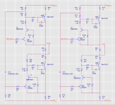
Most important is the wrong use of the gnd-tag.
It renders the left buffer branch, the com-buffer, useless.
What You named pgnd is actually gnd and vice versa.
gnd in LTSpice is a Reference fixed at a value of 0V.
The idea behind this circuit though is to create a 'floating' virtual gnd (Out_com) that's output offset equals the output offset of the main buffer(s).
As this virtual gnd buffer would be effected by the same power supply noise as the signal buffer, the noise would cancel if the load is connected between both their outputs.
In theory at least the quality of the power supply may then be low.
A smart idea, but it may present a couple of practical probs.
Both branches need to be precisely matched with regard to transistor parameters and temperature.
If not, the output potentials won't be equal and dc current would flow through the load.
Trimming of R8 and R2 would allow to adjust the output nodes of the two buffers at the same potential -preferrably 0V- but couldn't cope with temperature related offset drift.
The use of JFETs in the positive branch and bipolars in the negative ccs branch is prone to temperature related offset, as temperature gradients differ between transistor technologies and the bipolar 2-transistor ccs itself has its own temperature gradient.
This btw had been one important reason why I chose the same circuitry for positive and negative branch and recommended to match and thermally couple the two master JFETs.
The use of the ccs in the negative branch gives a high negative PSRR already, thereby reducing the quality requirement at least for the negative supply rail.
Probabely the PSRR even towards the positive rail is high enough to render the additional com-buffer obsolete.
Even though the RJM is a low parts number count circuit it requires increased effort for the additional buffer, effort in matching parts, and the cost of whole batches of parts to select from.
This effort imho surpasses that of adding good modern regulator chips and circuitry with lower requiremens regarding matching tolerances etc.
For a ultra-simple circuit supplied by a simple non-regulated supply it makes sense, but not for a already-increased-in-complexity circuit like Yours.
jauu
Calvin
if You wanted to copy the functionality of the RJM circuit You made a failure.
Most important is the wrong use of the gnd-tag.
It renders the left buffer branch, the com-buffer, useless.
What You named pgnd is actually gnd and vice versa.
gnd in LTSpice is a Reference fixed at a value of 0V.
The idea behind this circuit though is to create a 'floating' virtual gnd (Out_com) that's output offset equals the output offset of the main buffer(s).
As this virtual gnd buffer would be effected by the same power supply noise as the signal buffer, the noise would cancel if the load is connected between both their outputs.
In theory at least the quality of the power supply may then be low.
A smart idea, but it may present a couple of practical probs.
Both branches need to be precisely matched with regard to transistor parameters and temperature.
If not, the output potentials won't be equal and dc current would flow through the load.
Trimming of R8 and R2 would allow to adjust the output nodes of the two buffers at the same potential -preferrably 0V- but couldn't cope with temperature related offset drift.
The use of JFETs in the positive branch and bipolars in the negative ccs branch is prone to temperature related offset, as temperature gradients differ between transistor technologies and the bipolar 2-transistor ccs itself has its own temperature gradient.
This btw had been one important reason why I chose the same circuitry for positive and negative branch and recommended to match and thermally couple the two master JFETs.
The use of the ccs in the negative branch gives a high negative PSRR already, thereby reducing the quality requirement at least for the negative supply rail.
Probabely the PSRR even towards the positive rail is high enough to render the additional com-buffer obsolete.
Even though the RJM is a low parts number count circuit it requires increased effort for the additional buffer, effort in matching parts, and the cost of whole batches of parts to select from.
This effort imho surpasses that of adding good modern regulator chips and circuitry with lower requiremens regarding matching tolerances etc.
For a ultra-simple circuit supplied by a simple non-regulated supply it makes sense, but not for a already-increased-in-complexity circuit like Yours.
jauu
Calvin
Last edited:
you need the SAME quiescent current through the upper and lower halves, at all operating temperatures.
The lower CCS needs to be set up to minimise the output offset when there is no load.
Then you need to find the tempco that maintains this zero output offset for all operating conditions/temperatures.
Mixing BJT with jFET makes this almost impossible.
Use the same cascoded jFET for both the upper and lower cells.
Just a question:
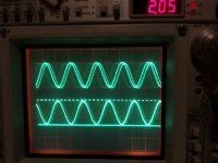
Does anybody know why or, if it is normal, but I am sure it's not, why the buffer (Calvin) saturates at -5V with Supply at +/-30V?
It seems it can't swing sufficiently high and I tried everything, at least that I know of.
I have bjt version with voltage divider on upper side and capacitor connected there.
Any help will be very appreciated.
Problem fixed, thx anyway!
I hv a different question, more of a curiosity than anything else: I think initially when this buffer was first designed, the mosfet version was compared against the BJT's by Mr. Joachim.
Did anybody else also did more test to evaluate which one sounds better?
I hv a different question, more of a curiosity than anything else: I think initially when this buffer was first designed, the mosfet version was compared against the BJT's by Mr. Joachim.
Did anybody else also did more test to evaluate which one sounds better?
Yes Calvin, I had already gotten rid of that, as you mentioned they only steal headroom.
One observation on the buffer: I tried it out in the past in my linestage inside a feedback loop and apparently there was no way to get it stable.
I wonder if anybody had th same experience. I had to end up settling fown for a different buffer.
Lasr: have you ever had a chance to compare MOSFET version with bjt's? If so which one sounded better to you?
Calvin Buffer question
Today I have a small question and some nice information.
I'm using the Calvin Buffer in my Paradise Phono and some 2 years ago I build the Calvin buffer pre-amp with it also. I use the seperate shunt PSU which was also used by the Paradise Phono.
My question is: do I need a capacitor on the PSU plus and minus between the shunt PSU and the Calvin Buffer? (see pic)
Some other information I will also give here.
I've used the Calvin Buffer with shunt PSU and a PSU with LM317/337 stuff for the shunt voltage input for a long time and was happy with it, till I had a McIntosh C39 in my system, which was a little better sounding.
I then build a PSU like the Prereg from the Paradise (double transfomers, skottky diodes, CLCRC and that was a very good step up....
I used a blue Alps pot for the volume and wanted a remote control for the Calvin Buffer.
I searched the net and came to the Muses 72320 chip. After some research I ordered the MCU and VCM boards from Academy Audio.
This week I just changed the Alps to the Muses and there is an incredible opening of the soundstage. Never expected it to be this much better. Now focus is extremely good, with very good separation of instruments, still very dynamic, which is a big plus of the Calvin Buffer, soundstage depth increased and most noticable in the bass. There is much more bass and goes much deeper and there is a lot of detail in the bass.
As you notice, I'm impressed
I will post pictures of my build when I finish it, now it's in a shoe-box.
Thx Calvin for this very good buffer
Attachments


I meesed up the ground connection and possibly damaged the jfets.CHANGED ALL JFETS out ,still getting 0.3 to 0.5V DC at output.
Second time it started with near zero DC at output and then temp of Jfets started going up and reached 35 degree and again showed 4V DC ,PERHAPS DAMAGED JFETS AGAIN.
Added some heatsinking and checked again.0.3V DC at out put with lot of oscillationslikely from heatsink picking up something.
Second time it started with near zero DC at output and then temp of Jfets started going up and reached 35 degree and again showed 4V DC ,PERHAPS DAMAGED JFETS AGAIN.
Added some heatsinking and checked again.0.3V DC at out put with lot of oscillationslikely from heatsink picking up something.
Correction to 0.1 mA IDSs.Started at 200mV. Eventually settled at 100mV. I am not sure if the drain resistors are too low or something, but again it’s a different design than running JFEts a IDSS I guess.
The bF862 are matched to 0.1 mA IDSS.
At one point I saw 20mV offset and I was happy, then ☹️
Attachments
Last edited:
JFETs: The New Frontier, Part 2 | audioXpress
Well , once read and forgotten article.
It seems like PMBF4392 is sufficient for cascode. VPinch off voltage is -5V and BF862 have it in the range of -0.8V.
Also I might be using too low of a source resistor .
As our beloved member Andrew once suggested in this article by Feucht
https://www.diyaudio.com/forums/att...492790608-pass-b1-pre-bf862-feucht-buffer-pdf
From data sheet and from the article from hifisonix linked below ( my batch has IDSs average about 14mA) I would select 9mA for 4 mA headroom to drive 5K load.
I would calculate a working voltage of 0.25V and working current of 9mA, then Rs should be about 28R.
I would assume to reduce the offset I would need to trim the lower resistor as again suggested by AndrewT.
Pass B1 pre with BF862.
http://hifisonix.com/wordpress/wp-content/uploads/2015/01/UBx.pdf
Last edited:
- Home
- Source & Line
- Analog Line Level
- Preamp-Buffers - simple idea